How to Ensure PCB Impedance Control During Routing
High speed signals and high frequency signals both have one thing in common: the need for impedance controlled routing on low loss, low dispersion interconnects. PCB impedance control can be difficult to achieve without the right set of routing tools and an integrated impedance calculator in your design tools. Most impedance calculators use a basic equation that does not accurately represent real traces on PCB substrates and does not correctly describe signal propagation.
Instead of risking your board’s functionality to sub-standard PCB design features, you need the best set of high speed design utilities you can get. The best PCB design software includes an accurate PCB impedance calculator that accounts for the material properties of real PCB substrates. These tools should also integrate with the rest of your schematic and PCB layout features to help you route high quality circuit boards. With an integrated software package, you can ensure PCB impedance control and stay productive.
ALTIUM DESIGNER
A unified PCB design application with a full suite of controlled impedance routing features for professional designers.
All high speed circuit boards and RF circuit boards need extremely accurate routing to ensure signals in the board will reach their destination. High speed/RF designers should know that designing to the correct impedance is vital in a circuit board. All interconnects that carry high speed signals must have the correct trace impedance to ensure power is transferred to load components without strong reflections.
Before you layout your next PCB design, check to see if you need controlled impedance and how to calculate it. You can calculate PCB impedance by hand, but it is easiest to calculate when you use the best set of PCB routing tools to create your layout. To really see where PCB routing features fit into the controlled impedance landscape, it helps to understand how impedance is calculated and what most PCB impedance control calculators can’t do.
PCB Trace Impedance Calculations
There are a few methods for calculating trace impedance in a circuit board as long as the dielectric constant and trace geometry are known:
- Use the IPC-2141 equation for microstrip or stripline impedances
- Use Waddel’s transmission line equations
- Use a field solver that can account for dispersion and copper roughness
Most trace impedance calculators are based on the IPC-2141 method, which is known to be inaccurate for today’s modern high speed/high frequency PCB designs. Waddel’s equations are widely regarded as the most accurate analytical tools for calculating impedance, but they are difficult to use for PCB impedance control. This is because a numerical algorithm is needed to solve these equations to determine the best PCB trace width needed to reach an impedance target.
Instead of these methods, your PCB design tools should include features that can automatically calculate the trace width required to reach an impedance target.
Include Dispersion and Loss in Impedance Calculations
Real PCB laminates have some loss, copper roughness, and dispersion that need to be included in an impedance calculation. Accounting for loss and dispersion is easy when you have access to PCB design tools with an integrated field solver for impedance calculations. With the design tools in Altium Designer, you can easily calculate the impedance you need without using complex models or equations, and you can start routing your board to comply with your impedance profile.
- All loss sources should be included in your PCB impedance calculations to ensure accurate impedance control.
Learn more about loss and dispersion in your circuit board layout.
- The best PCB impedance control calculators can account for dispersion in the laminate material, giving highly accurate impedance calculations over a broad frequency range.
Learn more about dispersion in FR4 laminates and other PCB substrates.
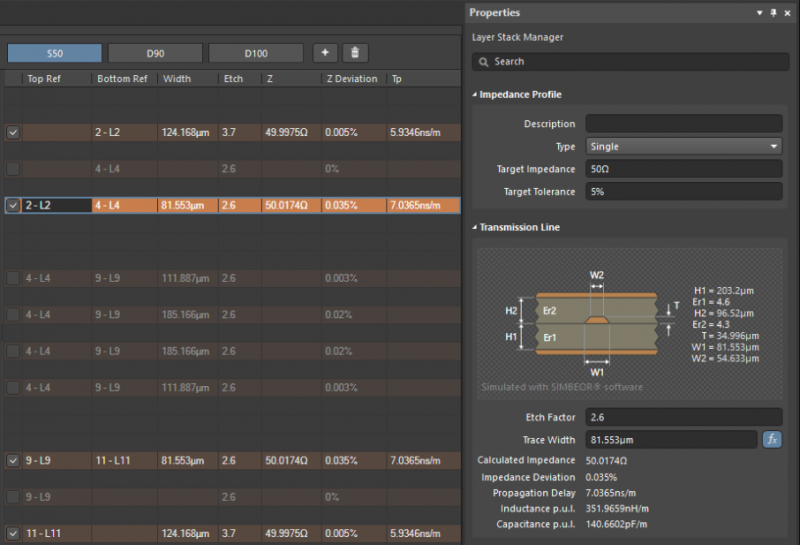
- Altium Designer’s Layer Stack Manager includes the impedance calculation tools you need to ensure controlled impedance routing.
Learn more about using the Layer Stack Manager in Altium Designer.

High speed PCB design and routing starts with creating a PCB stackup that enables impedance control.
Accurate Impedance Controlled Routing
Once you’ve calculated the PCB trace width needed for impedance control, your routing tools need to apply that width automatically in your PCB layout. Most design tools force you to do this by hand, making it difficult to guarantee accuracy. The fastest way to create impedance controlled interconnects is to use the best set of routing tools with a rules-driven design engine to ensure impedance goals are met.
The rules-driven design engine in Altium Designer does exactly this, while other impedance calculators can’t pass calculation results directly to your routing tools. When your high speed routing features can automatically take your PCB design data and apply impedance targets as a design rule, controlled impedance routing is much easier and more accurate.
Guarantee PCB Impedance Control with Altium Designer
Instead of taking your chances and using a calculator that gives incorrect results, use the best set of impedance controlled routing tools in Altium Designer. The power of Altium Designer for high speed PCB design comes from its integrated interface, where the PCB routing tools take data directly from an integrated field solver and use it to set your controlled impedance value as a design rule. With this type of application, it’s easy to ensure PCB impedance control as you create your layout.
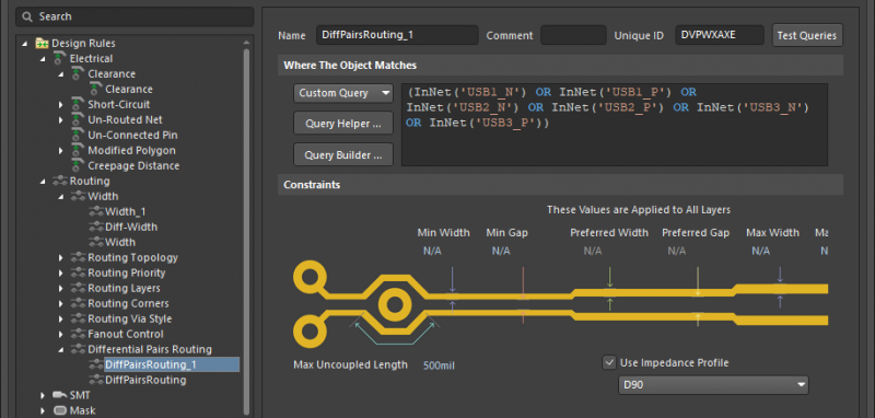
- Setting up impedance limits as design rules is easy when you use Altium Designer’s integrated impedance calculator and interactive routing tools.
Learn more about Altium Designer’s interactive controlled impedance routing features.
- Altium Designer’s routing tools will let you apply length matching structures like serpentine and switchback routing.
Learn more about controlled impedance routing with length matching.
- There are some other important high speed routing constraints that you’ll need to consider, and Altium Designer can help you satisfy all of these and many more.
Learn more about high speed PCB routing rules and constraints.

Altium Designer’s rules-driven design environment lets you apply impedance profiles to your high speed interconnects.
How Your Software Uses PCB Impedance Control Calculations
Your controlled impedance designs don’t need to be difficult when you have the best set of routing and layout features in a single program. Creating a high quality PCB layout starts with the right design engine to help you stay productive.
The rules-driven design engine in Altium Designer unifies every design tool you need for controlled impedance routing and layout into a single application. The real strength of Altium Designer is its rules-driven design engine, which checks your layout against basic and advanced design rules as it’s created. This helps ensure high accuracy and conformance to design requirements.
Everything You Need for Controlled Impedance Design
When you need to create high-quality PCB layouts, don’t settle for design platforms that piece together multiple tools from different vendors. Everything you need for design, layout, component sourcing, and manufacturing can be found in Altium Designer’s unified environment. You can stay productive and ensure ultra-accurate impedance controlled routing in Altium Designer.
- Altium Designer includes everything needed to design simple circuit boards and advanced high speed PCBs in a single application.
Learn more about the unified design environment in Altium Designer.
- The integrated field solver from Simberian interfaces directly with the Layer Stack Manager in Altium Designer, giving designers an integrated tool for accurate impedance calculations.
Learn more about the integrated field solver from Simberian in Altium Designer.
- When you’re ready to share your project with other PCB designers or your manufacturer, Altium 365 lets you instantly share your circuit board design and production data through Altium Designer or on the web.
Learn more about sharing your PCB project data with Altium 365.

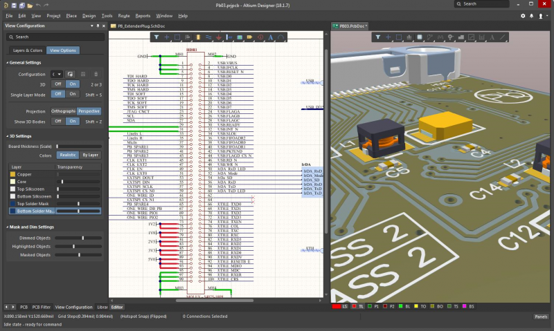
Layout your impedance controlled high speed PCB design with ease in Altium Designer.
PCB impedance control shouldn’t be difficult. Instead of trying an external calculator, use the complete set of stackup design, impedance calculation, and interactive routing features in Altium Designer. You can stay productive while designing high frequency systems and preparing for manufacturing when you use Altium Designer.
Altium Designer on Altium 365 delivers unprecedented integration to the electronics industry until now relegated to the world of software development, allowing designers to work from home and reach unprecedented levels of efficiency.
We have only scratched the surface of what is possible to do with Altium Designer on Altium 365. You can check theproduct page for a more in-depth feature description or one of theOn-Demand Webinars.
