Pandemic PCB Prototyping: Building Electronics From Your Living Room
It feels like everyone is writing an article these days about how they’re managing (or not managing) with stay-at-home orders due to COVID-19 restrictions. At the time of writing, California (where I am based) has the highest number of cases over any other state in the United States. To combat the pandemic, most non-essential businesses have been closed or open in a limited fashion. This means that folks who are able to work from home (e.g. Engineers) are encouraged to do so. This also means that engineers who are used to their full lab setup at work now find themselves creating makeshift ones at home. I, for one, enjoy and appreciate the opportunity to be at home with my family, but soldering at the dining table next to my curious four-year-old doesn’t exactly give me warm fuzzies. In this article, I will be discussing how to most effectively get your PCB prototyping “hackerspace” up and running, where to cut corners, and when to spend the dough.
The Project
Over the past few months during California’s stay at home orders, I have embarked on retrofitting our ceramic kiln with an electronic kiln controller. There are countless DIY reflow oven projects out there, and the kiln controllers are extremely similar (some folks even forked and repurposed reflow oven repositories for this reason). The one main difference between a kiln and a reflow oven is temperature: kilns get really hot. As I embarked on this DIY project, I threw together a prototype very quickly (as most of the code can be found online). It ended up looking like this:
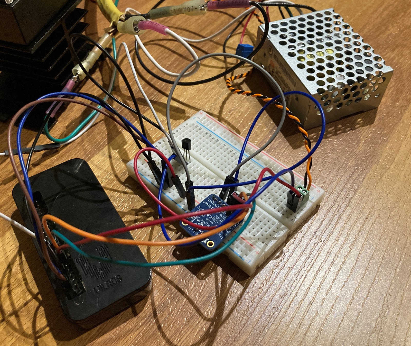
Of course, this setup was hacker status (at best), but it gave me a proof of concept. Now what I needed was to create a neatly packaged controller without breaking the bank.
Materials and Equipment for PCB Prototyping
Given the fact that I didn’t have access to a full-on lab for PCB prototyping, I had to get creative for my setup at home. It’s a fine balance between what is nice to have and what is a need to have when it comes to lab equipment. It’s also easy to overspend in this area because these are the things engineers like to refer to as “toys.” The first step is getting a feel for what you’ll actually be building. For example, if you know you’ll be soldering a few through-hole resistors and a large IC onto a PCB, then you probably don’t need to splurge on a costly soldering iron. I’m sure I’m going to get a lot of slack for this later, but I will say that my $20 soldering iron has worked just fine for me (albeit I don’t solder anything with it that’s smaller than 0603s). If you’re going to invest very little in your soldering iron, you need to be strategic about what parts you choose for your first prototype. For PCB prototyping on a shoestring, I generally follow this flow:
- Build a prototype with a solderless breadboard (or a solderable one) and jumper wires.
- Design a PCB using parts you know you’ll be able to solder yourself (via low-cost PCB fabricators such as OSH Park). Stuff the board yourself with through-hole parts or ones with large surface mount pads.
- Spin the next iteration of your PCB using small surface-mount parts with a low-cost fab/assembly house (such as CircuitHub or PCBWay).
For board bring up you’re also going to need a decent power supply and maybe an oscilloscope or logic analyzer. There are plenty of low-cost solutions out there. At the time of writing, you could find decent 300W power supplies for less than $100. For oscilloscopes and logic analyzers, you could also find something reasonable for low-speed applications priced under $200. My favourite is the Analog Discovery 2 which is priced just under $300 at the time of writing. If you’re going to need more power or an oscilloscope that offers higher bandwidth and sampling speed, then you will have to invest a bit more in your equipment.
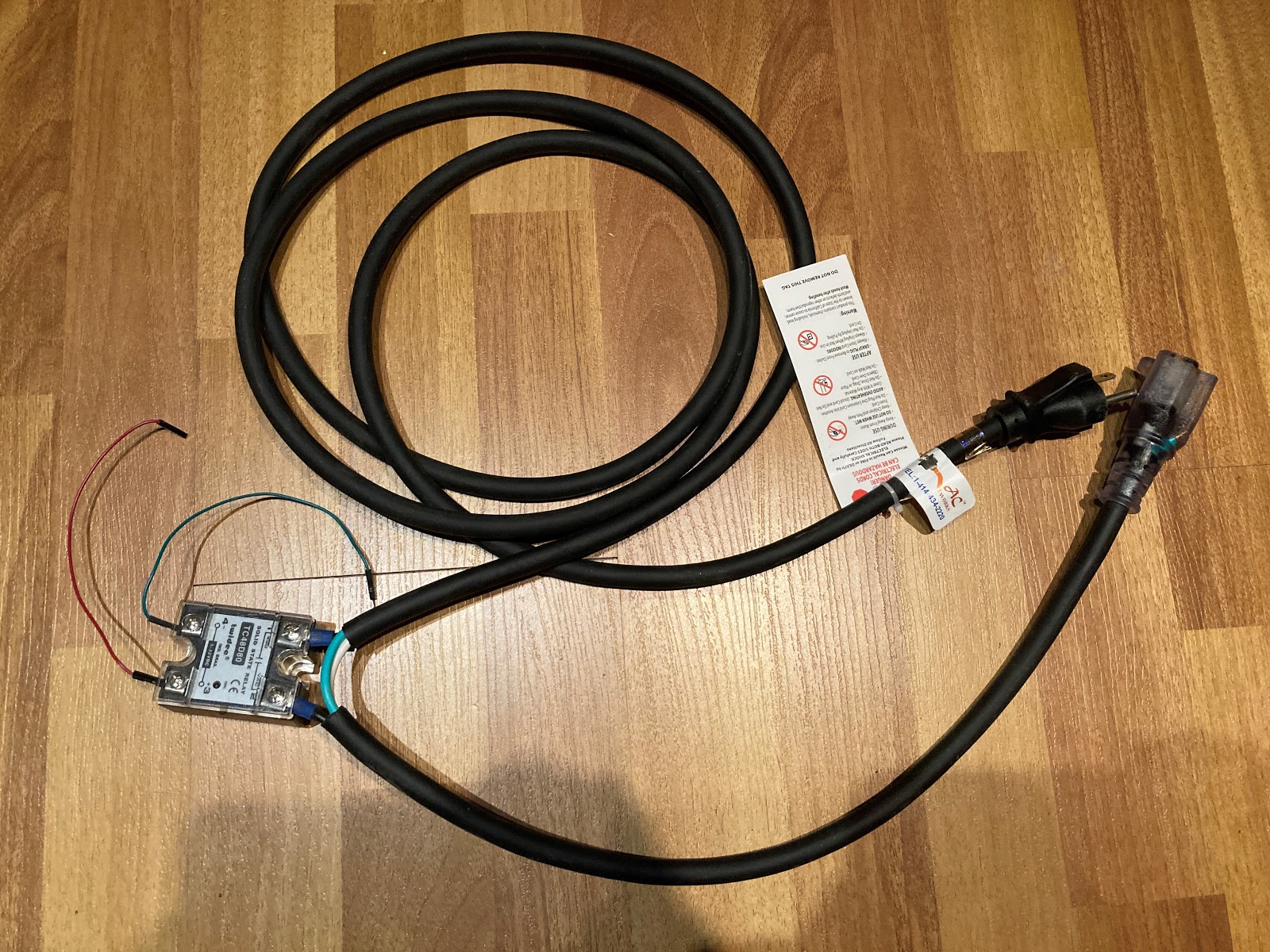
Another area that can sometimes get overlooked in PCB prototyping is cabling. In my case, I am working with 120 Volts (AC) at 20 Amps. This can be lethal if not handled properly. One of the most obvious precautions you can take (but often overlooked) is not leaving around exposed wires. Even when you are just hacking on electronics, this can save an IC from frying or you...from dying. Again, we are prototyping at home, so we don’t have the luxury for fancy connectors that require expensive crimpers. I decided to work with what I could find at the local hardware store. In my first example, I’ve purchased an extension cord and spliced out the hot wire to insert a solid-state relay inline. Rather than take the wire directly and insert it into the screw terminal I’ve put a fork lug on it and then attached it. I also do this with low voltage wires as well. It’s inexpensive and gives it a more polished look without much effort.
Another great way of creating a low-cost, minimal effort cabling is making use of quick connect spade lugs. I needed the ability to disconnect and reconnect my AC to DC power converter, so I slapped these on with one end as 12 AWG Romex and the other 18 AWG stranded wire:
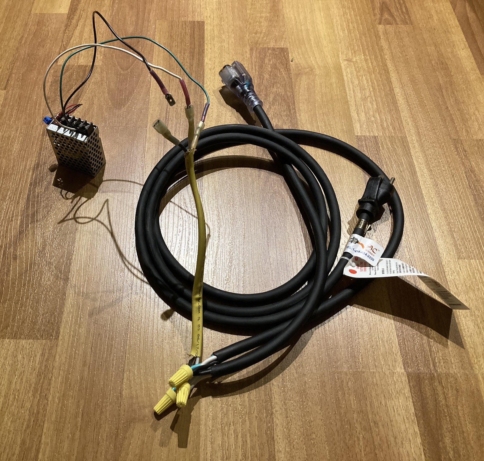
You will also notice the wire twist caps. That’s definitely hacker status but cheap, quick, and relatively safe. I considered going with terminal blocks, but this was the most straightforward option (at such a high current).
From Maker to Pro
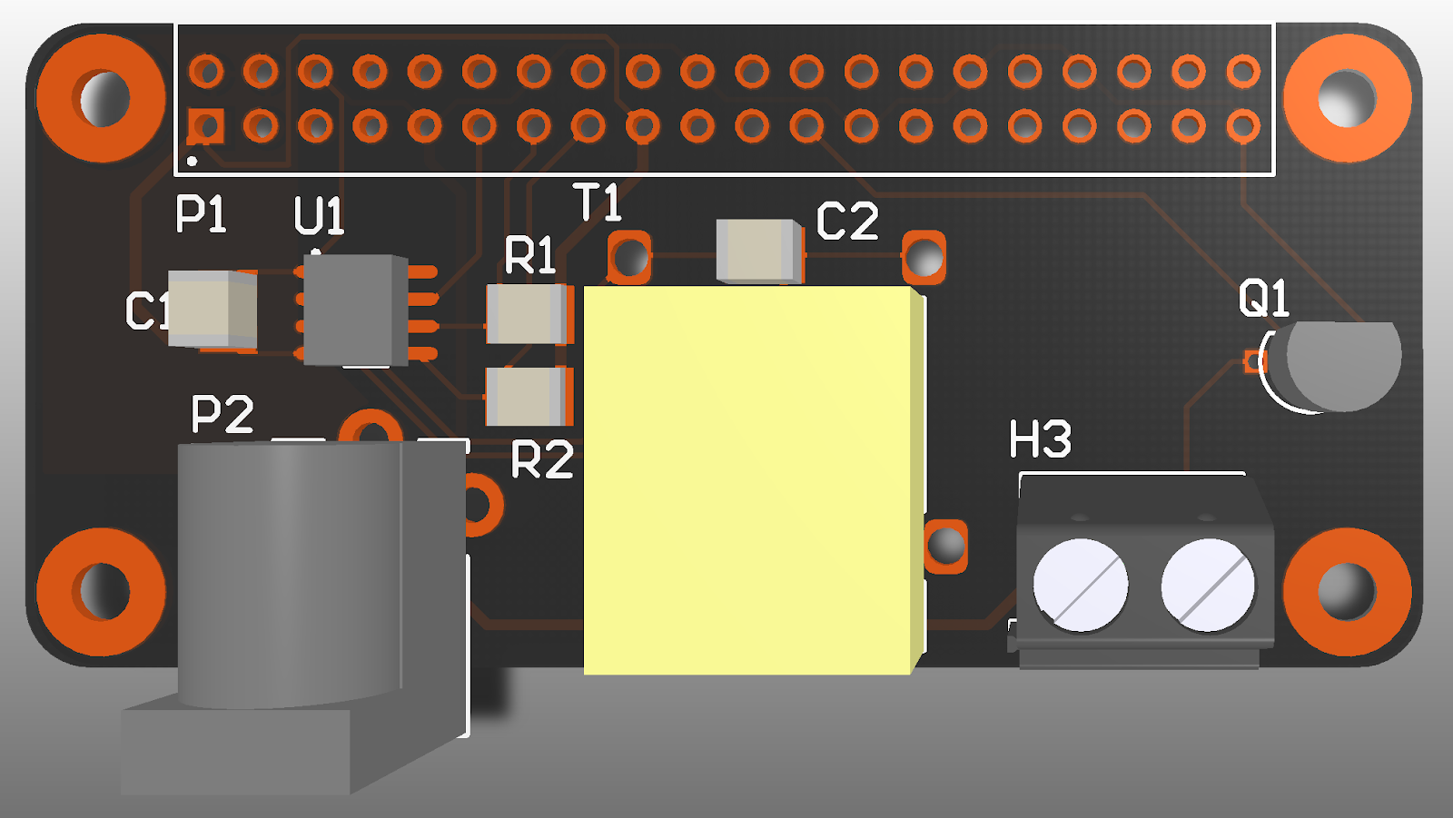
So you’ve built your prototype, and now you’re ready to give it a polished look. Let’s go back to the discussion of spinning the low-cost PCB. It’s essential to compare purchasing off the shelf evaluation boards versus spinning one yourself. You can get a very polished and clean look just by using evaluation boards with slight modifications. This is especially important when you’re low on time and components are too small to solder yourself (or they require lots of support circuitry like an FPGA or microprocessor). Another consideration would be to purchase System on modules which put together all the necessary supporting circuitry for those complicated microprocessors and FPGAs but then expose many extra pins for you to hook up your other circuitry to. If you’re up for it, getting a cheap PCB made and/or having it stuffed can be quite reasonable (depending on the complexity of the board). Suppose you’re building off of a PCB prototyping platform such as a Raspberry Pi or BeagleBoard. In that case, there are countless designs in the CircuitMaker community that can be easily imported into Altium Designer® to get you started. With the Octopart® footprint integration in Altium Designer, it’s even easier to get the components that you need without spending all those extra hours designing footprints.
Here is the final design of the board that replaces all of the breadboard wires that you saw in Figure 1:
_10.png)
The most important point I’d like to stress here is the “good enough” principle. We are designing a prototype board that gets rid of all those nasty wires - not a PCB going to space. There is a time and place for iterating many times over, but there is also a place for getting something out quick and cheap (especially for a low-cost prototype).
Conclusion
In this article, we reviewed some guidelines on PCB prototyping while sheltering in place during these difficult times. These guidelines included different techniques used within my hobby project, demonstrated with examples. We also briefly discussed the need and nice to haves of equipment for prototyping at home. Most importantly, the idea here is to have fun without breaking the bank (and without the need to replace your high-end lab at work).
Would you like to find out more about how Altium can help you with your next PCB design? Talk to an expert at Altium.