Noise Margin Analysis Part 2

Part 1 of this article addressed the three elements that comprise a design rule set, noise sources and their impact on a system’s overall operation including Vcc, and ground bounce and ground and Vcc offsets. Also described, was what needs to happen when current leads are so high that it’s not possible to put enough copper in the power path. This second part addresses further noise sources and their impacts, including ground and Vcc drops in IC package power leads; reference accuracy; signal losses in traces; thermal offsets and effects; and terminator noise and power supply variance. Also included are examples of noise margin analyses.
Ground and Vcc Drops in IC Package Power Leads
There is a non-zero resistance in the power leads of every IC package. The steady state current drawn by high power ICs will generate a DC voltage drop that will result in Vcc on the die being lower than Vcc on the power plane and ground on the die being higher than ground on the PCB. These DC offsets directly shift logic levels in such a way that the noise margin is eroded. It’s imperative that these offset voltages be quantified and allowances made for them as part of the noise margin analysis process. This offset can be calculated if the DC resistance of the power paths and the quiescent current draw are both known.
Reference Accuracy
Many logic families have internal reference voltage generators that are used to determine the threshold of voltage between the logic 1 and logic 0 levels. To the extent that the reference voltage drifts away from its design value either the logic 1 or logic 0 noise margin is eroded. Reference voltages can drift with temperature, time or changes in Vcc. Logic families with reference voltage generators include ECL, GTL, BTL and LVDS. Of these, only ECL shows significant drift with both changes in Vee (voltage at common emitter that is the negative supply voltage) or temperature. Noise margin allowance must be made for these expected changes in ECL logic devices.
Signal Losses in Traces
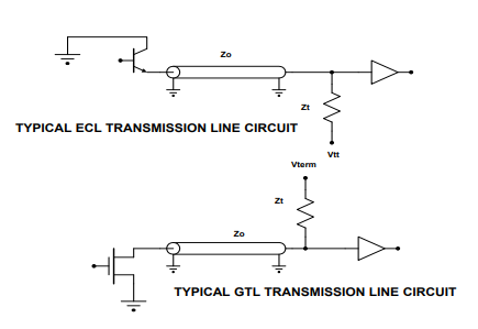
When parallel terminations are used at the load end of a net, there will be a quiescent current flowing in the transmission line. As shown in Figure 1, a voltage divider is formed by the trace DC resistance and the termination resistor.
This results in one of the logic levels at the loads being less than it should be. Some of the noise budget needs to be allocated for this erosion. Figure 2 is a plot of trace resistance versus trace width and trace thickness. As can be seen, for the narrow traces in thin copper, the resistance per unit length is quite significant.
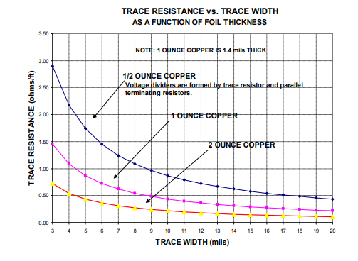
This combined with the fact that a typical GTL or BTL bus is less than 30 ohms, means that the signal loss may be substantial.
In addition to the DC resistance of a transmission line, skin effect loss will further erode the signal at the receiver. Since skin effect loss is frequency dependent—it’s not possible to perform simple calculations to find out how much signal erosion will occur as a result of this phenomenon. In order to assess this effect, it’s necessary to build a model of the circuit being examined and then make time domain measurements.
The modeling tool used for this purpose must be able to model transmission lines in three dimensions.
Howard Johnson’s book cited at the end of this article addresses skin effect losses and the physics behind them.
Thermal Offsets/Effects
The reference voltages and the values of the output voltages of some logic families are affected by changes in junction temperatures. As a result, allowances need to be made for this. The only logic family that has significant voltage shifts as a result of changes in temperature is ECL. The voltage levels of various MOS logic families are not significantly affected by temperature.
Terminator Noise
When there are large numbers of termination resistors in a design, it is common to use resistor packs that contain multiple resistors in one package. Figure 3 depicts this type of package.
_3.png)
When a logic signal terminates on one of these resistors switches, the change in flow associated with the logic change will develop a voltage drop across the inductance in the common backbone connection (parasitic inductance). This delta V will cause the common terminal of all of the other resistors to move, inducing a noise voltage on the logic lines in question. This noise is coupled through the common connection in the R-pack.
R-packs are not as commonly used in CMOS devices as they were with ECL ones. This is because CMOS circuits use series terminations that don’t have a common connection. Newer versions of DDR memory arrays are parallel terminated to a termination voltage that is Vdd/2. This termination voltage is created with a special voltage regulator. All of the parallel terminations are tied to a common node, such as that shown in Figure 3. It’s important that this connection be of very low inductance and that there is a very good plane capacitor attached to the node. This will provide the fast switching currents associated with this architecture. If this is not done, noise will be coupled signal-to-signal through this path, eroding signals to the point of failure.
Power Supply Variance
Power supply variance is comprised of three elements, including:
- Long term voltage drop.
- DC voltage drops across the power distribution system.
- Ripple associated with switching activities such as driving transmission lines as well as the standby to active changes associated with components such as microprocessors.
The component manufacturer’s data sheet will typically specify the total variation that a logic family can tolerate by summing up the foregoing elements. It follows that the tolerance specified will have to be “spent” on these three sources of erosion. It’s frequently assumed that the total variation is available for ripple but if this happens, it will result in an unstable system. As a result, it’s necessary to make tradeoffs between the weight of the copper in the distribution system, the quality of the voltage regulators, and the total decoupling needed to keep the ripple within limits.
It’s important to remember that with CMOS logic or any other logic that shorts an output line to the Vdd rail, all of the ripple that appears on Vcc or Vdd will appear unattenuated on the logic lines when the logic level is a 1. When one of these logic lines leaves the product, the ripple voltage on it will create EMI.
As a result, it’s important that the maximum allowable ripple be determined as part of the noise margin analysis that is outlined below. Failure to minimize high frequency ripple is a common cause of EMI.
Noise Margin Analysis Example
The example below shows how a design rule set is created using noise margin analysis. The proposed design rules will be examined to determine whether or not the design will function properly if the rules are used. If not, changes will be made until the total noise generated by all of the rules is within the noise margin of each family used. When the noise budget is balanced, the design rule set will result in a stable design.
The rule set being examined is that used to design a typical six-layer PCB as shown in Figure 4.
_1.png)
The routing rules allow 5-mil lines and 5-mil spaces. In this instance, the crosstalk on either outer layer could be as much as 34%, and on the inner layers, 25%. The impedance on the outer layers is 102 ohms, and on the inner layers is 70 ohms. The 5-volt CMOS logic is examined first. This logic family has a maximum signal swing of 4700 mV and a noise margin of 1000 mV. Table 1 lists the results of the noise margin analysis of this rule set.
_0.png)
As can be seen, the total noise exceeds the budget by 150%. If a system is designed with these rules, it is likely to be unstable. Therefore, it’s necessary to change the rules in order to reduce the total noise. These changes should be done in such a way as to minimize the total cost of the product. As shown, the two largest noise sources are crosstalk and reflections. A simple way to reduce both is to control impedance and reduce crosstalk by moving the trace layers closer to the planes. Restacking the PCB achieves this. For example, this has been done in the right side of Figure 4. The change adds no cost to the PCB, and the resulting noise margin analysis is provided in Table 2.
.png)
As can be seen, both the crosstalk and the reflections have been significantly reduced. However, there is still too much noise and crosstalk, and reflections continue to be the major sources of it, so they should be examined for further reductions. The amount of noise resulting from reflections is that which results from the +10% impedance tolerance that is the reasonable limit for the PCB fabrication process.
Reducing reflections below this limit will increase the cost of the PCB. However, further reducing crosstalk, within limits, will not add cost. This can be done by separating the traces and reducing the height of the trace above the nearest plane. Here, the trace-to-trace separation was raised from 5 mils to 8 mils. The results of this change are shown in Table 3.
_2.png)
After changing only two rules, neither of which added any cost to the design, the excess noise has been reduced from more than 1700 millivolts, to approximately 200 millivolts. At this stage of the design process, there are three significant noise producers. They include:
- Reflections
- These can be reduced without adding cost.
- Crosstalk
- This can be further reduced by increasing trace-to-trace spacing or reducing the height of the trace above the nearest plane.
- Vcc and ground bounce
- These will require a package change to reduce.
Whether further noise reduction is warranted depends on the final application of the design. It must be kept in mind that the underlying principle used in this analysis is that, on occasion, all of the noise sources will coincide to produce one large noise spike that can cause a failure. The more complex the system, the more likely this is to occur. Conversely, the simpler the system, the less likely this will occur. If the product in question is a video game and a failure occurs, only the player is inconvenienced. If the product in question is a terabit router, it is more likely that such a failure will cause major damage.
At this point in time, it’s necessary to use engineering judgment to determine if more cost should be incurred to further reduce noise sources. If the product is a simple dual-speed Ethernet hub, it’s reasonable to stop at this point and design the product. When this decision is made, every design rule needed to create a stable product has been determined and routing of the PCB(s) can proceed.
It should be noted that all of the design rules have been established before a single PCB has been designed, and the first schematic drawn. It is both possible and vital to develop all of the design rules early on in the design process.
Table 4 presents the same analysis as that shown in Table 2 but with a GTL bus data. As can be seen, the noise swings are very small (800mV) and the noise margin is 370 mV which is almost half of the signal swing.
.png)
This large ratio of noise margin to signal swing is the mark of a well-designed logic family. Without any extra effort, the noise budget is almost balanced. With a major change in spacing, crosstalk could be reduced enough to achieve balance. It should also be noted that there is no allowance for power supply variance. This is because the outputs of BTL and GTL logic are parallel terminated to a termination voltage that is independent of Vdd, which can be more tightly controlled as it only supplies power to the pull up resistors.
Recording the Design Rules
Once the design rules have been developed it’s necessary to record them in a way that makes it easy for the design team to use. Table 5 presents one method for doing this. In most systems, this is referred to as the technology table.
.png)
The concept here is that most designs can be partitioned into a limited number of net classes. All of the members of a given class require the same design rules. Once the net list has been partitioned into its classes, labels are given to each class, and those labels are then added to the net list.
Schematic tools used for this class of design have a field within them that can be loaded to these labels. PCB layout tools intended for high speed designs have the ability to interpret the rules set forth in the technology table, and can route traces to them. These rules are all geometric and include length, trace width and trace spacing. With this kind of layout tool, there is no need to do real time analysis of the traces during routing. In addition, when routing has been completed, post-rout analysis consists of checking these same geometries. There is no need to do post-route board-level signal integrity analysis.
This maximizes the effectiveness of design rule creation and reinforces the objective of achieving a design that works right the first time.
Summary
Noise margin analysis is the systematic examination of design rules to ensure the total noise does not violate the margins of all the logic circuits in a design. It is a relatively simple process that should be performed before the design process starts. Failure to form this analysis commonly results in unstable designs. Troubleshooting an unstable design takes far longer than does performing noise margin analysis. Furthermore, a properly developed noise margin analysis will ensure that a design will work right the first time and every time thereafter.
Have more questions? Call an expert at Altium or continue reading about adopting signal integrity in your high-speed design process.
References:
- Ritchey, Lee W. and Zasio, John J., “Right The First Time, A Practical Handbook on High-Speed PCB and System Design, Volume 1.”
- Johnson, Howard, “High Speed Digital Design: A Handbook of Black Magic”.