How to Navigate the Perils of PCB Design Review
Whether you’re a first-time designer or a hardened veteran, the integrity of your designs relies heavily on inspecting a product for design errors before production. What can be done to identify design flaws while staying productive? Before a new design is sent into production, it's critical to put the design through a PCB design review so that design errors can be identified before manufacturing. In many cases, a design will pass rules checks perfectly, yet it can fail to get through manufacturing without defects, so designers still need to check all aspects of a design before sending it in for manufacturing.
What can be done to reduce the risk and of a failed fabrication run and ensure your designs are free of defects before heading to manufacturing? The right PCB design software not only helps you create your design, it can help you collaborate with your team and manufacturer to get through a design review quickly. You'll need the design tools inside your PCB layout software, as well as the collaboration and sharing features in Altium 365 to help you pass a design review.
What to Look For in Your PCB Design Review Process
There is a list of important features to check in your PCB design review process. Some of these points can be checked automatically in your DRC engine, while others need to be checked manually. It's important to remember that there are many electrically or functionally incorrect design choices that will still pass design rule checks. The converse is also true; there are electrically correct (and intentional) design choices that will violate a design rule check. Make sure to keep your list of functional requirements compiled in a checklist and look at all of these points during a design review.
Here are some of the most important points to check during a design review:
- Board thickness (you'd be surprised how often this is overlooked)
- Sufficient ground pour to provide shielding and low-impedance return paths
- Grouping and clearances for critical components
- Interconnects: Trace widths, via counts, total trace length, and clearance to planes
- Differential pairs and parallel buses: Trace spacing and length matching
- Impedance calculations
- Stackup construction and material specifications
- Edge and housing clearances for connectors, heat sinks, and other large components
All of these points are very important, but the only points that can be checked automatically in your DRC engine are interconnect geometry/spacing, trace impedance values (NOT plane impedances), and clearances. The other points require some manual checks. There are also product-specific points and standards that should be checked in the design, both with your team and with your manufacturer.
Tools for Working a PCB Design Review
DRCs were mentioned above, but designs teams and their manufacturing partners still need ways to collaborate on design reviews, particularly for anything that requires manual inspection. The best design software makes it easy to quickly scan through a PCB layout and zoom into areas that might require deeper inspection.
Filtering in Your PCB Layout
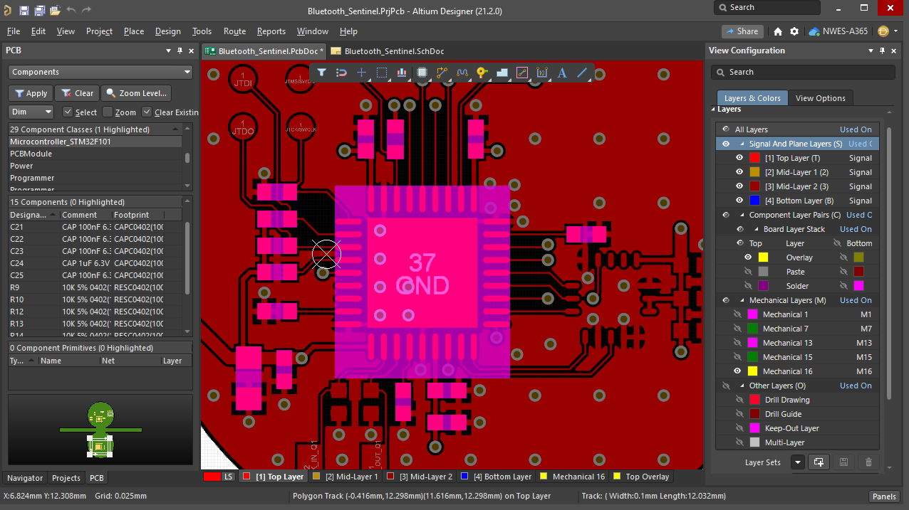
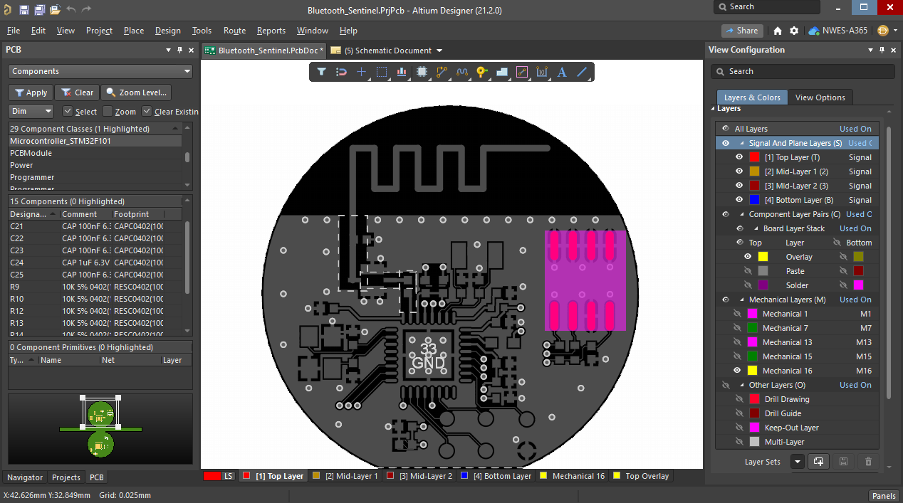
Finding a component in your layout can sometimes be cumbersome, especially if you don’t know what other components should be connected with that specific component. Altium Designer provides a solution where users can easily customize the view filtering options to only show necessary components on the PCB. This makes it easier to navigate to specific features in the PCB layout during a design review.
Comparing Gerbers and the PCB Layout
A conscientious manufacturer will check your Gerbers before fabrication to ensure your layout matches your fabrication data. PCB design tools with an integrated CAM viewer and editor allows a manufacturer to open and view Gerber files, which can then be compared with the PCB layout in the same program. Altium Designer's CAMtastic tool provides this functionality for Gerber RS-274-X and X2 files, which allows any Gerber errors to be quickly spotted and corrected.
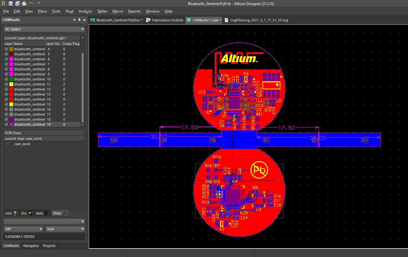
The best way to ensure your Gerbers and PCB layout always match is to simply regenerate the Gerbers instantly within your PCB design tools. If you created an OutJob file in your Altium Designer project, you can recreate your Gerbers in a matter of seconds. Don't fret with modifying your Gerbers each time the layout is modified, you can quickly regenerate your fabrication data and release it to your manufacturer to continue the review process.
Automated Board Reports
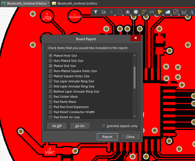
One quick way to scan through a long list of design requirements is to compile board features and measurements into different reports. Altium Designer makes it easy to generate these reports directly from within your PCB layout. Dozens of features can be examined and a report can be generated from a single window, as shown below. This is a great way to generate a summary for a customer who is concerned about adhering to specific design standards or signaling standards.
Sharing Through the Cloud with Altium 365
Altium 365 is the newest tool that helps design teams share and collaborate on PCB design projects. Because entire projects and fabrication/assembly data can be shared directly from Altium Designer into Altium 365, it's easy for a design team and a manufacturer to collaborate on a PCB design review. Once a project is shared into Altium 365, it can be accessed through a secure web platform, just like you would access shared documents on Google Drive or other cloud platforms.
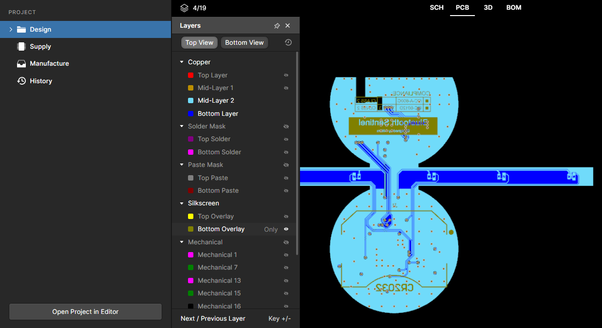
Placing your projects on a managed cloud server through Altium 365 provides many other benefits you won't find in other cloud services. Design teams can easily collaborate and manage their design data within Altium Designer or in a dedicated Workspace in their web browser. Designers also have access to the following features for data management:
- An integrated revision tracking and version control system
- Control over user access, viewing, and editing privileges for files and projects
- Component, project, and library management features
- Sharing features that allow a design to be instantly sent to a manufacturer
Collaborate on PCB Design Reviews with Altium 365
Every design team is different, and manufacturers may have their own DFM tools they use to ensure manufacturability. Both groups can come together and collaborate on PCB design reviews with the Altium 365 platform, which makes it easy to spot and correct design choices that affect manufacturability and product functionality.
If your team wants a new way to get through a PCB design review before manufacturing, use the sharing and collaboration tools in the Altium 365™ platform. Any project or fabrication release that is shared through Altium 365 can be opened, reviewed, and edited in Altium Designer®, giving remote design teams and manufacturers a seamless way to collaborate on complex designs.