How to Create a Planar Transformer PCB Layout

By far, the bulkiest through-hole component you can place on your PCB is a transformer. The only comparably large components I can think at the moment of our large high voltage capacitors, wire-wound inductors, some connectors, and heatsinks. Even small transformers take up more space than the majority of integrated circuits, and power system designers need to carefully consider the size of these components when creating a PCB layout.
Through-hole mountable transformers can sit very tall on the PCB, so it helps to have an alternative that has a low profile. A planar transformer is one option that can be through-hole mounted to the board, or it can be integrated directly into your PCB. Both options give you a low-profile transformer that could handle a range of current values. Here’s how you can create a planar transformer PCB layout.
What is a Planar Transformer?
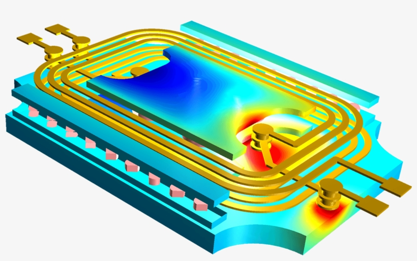
A planar transformer uses flat windings that can be placed directly on a PCB. Contrast this with a toroidal transformer, laminated core transformer, or other common transformers, where copper wire is used to form the windings around the transformer core. Using a PCB with traces to form the windings creates the planar form factor. Thanks to the form factor and materials used in the transformer, it has some advantages compared to other transformers:
- Low profile. These transformers aren’t as tall as other transformers with similar specs. This can give a sleek design for thin enclosures.
- High heat dissipation. Having a low profile spreads out the transformer over a wider area. Although this means the transformer takes up more board space, more heat can be dissipated from the transformer during operation.
- High efficiency. The compact design of these transformers reduces leakage inductance, so planar transformers have very high efficiency. Typical values top 99%.
- Low stray intra-winding capacitance. The stray capacitance within a winding can be made quite low by placing the inputs and outputs far from each other on the board.
There are also some tradeoffs to consider if you’re designing a custom planar transformer, or you want to integrate a planar transformer into your PCB layout:
- Limited current capacity. Since planar traces are used to form windings, they need to be designed to ensure sufficiently low-temperature rise. High current limit means the transformer needs to be designed to have more board space. Take a look at the IPC-2152 standards for more information.
- Limited turns ratio. The trace width requirements for different current ratings and any limit you might need on footprint size can limit the number of turns you can place on the PCB.
- Higher tooling investment. Standard transformers use readily available materials, whereas a planar transformer requires putting the component through the standard PCB fabrication process.
- High stray interwinding capacitance. The stray capacitance between windings can be rather high due to the arrangement of coils on different layers of the PCB.

Designing a Planar Transformer in a PCB Layout
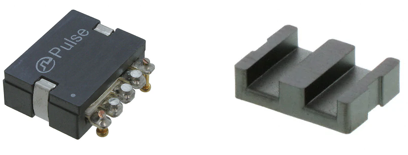
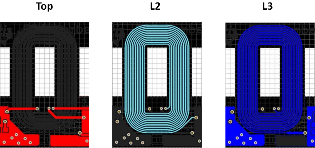
As was mentioned above, there are two ways to build a planar transformer: as its own component or integrated into a larger PCB layout. Both types of planar transformer follow the same process. The example layout below shows how a planar transformer is formed by wrapping the transformer core material around the PCB layout using cutouts. The two sides of the core can be screwed together or secured with a small clip, as shown above.
In the example design below, the traces in each layer are routed in the desired shape of the coils, as well as the input/output ports for each winding. You can easily put multiple primary/secondary windings in the layout. Although this is normally done on its own component, you could also do this on the same board as the rest of your components, which gives you a fully integrated package.

In addition to the points mentioned above, pay attention to these two points when designing a planar transformer:
- Layer stackup. You also need to select the proper dielectric thickness between in the board stackup. The thickness of the dielectric determines the stray capacitance between the windings, the maximum voltage (due to breakdown), and how fast heat can be dissipated.
- Frequency. Planar transformers are normally used with ~kHz frequencies. To prevent capacitive leakage across the windings, or between planes near the transformer coils, the capacitance can’t be too large.
There is a delicate balance involved in designing these components. We can’t make the current too large as this requires wider traces; this then increases the capacitive coupling, which limits the usable frequency. We also can’t have large step-down values; commercial planar transformers can have ~6:1 turns ratio, although the inductance can be quite high and reach up to ~1 mH levels.
Routing the trace coils with curved shape or other geometry requires arc routing or any-angle routing to place PCB traces accurately. Then there’s the matter of heat dissipation from the transformer going back into the substrate. There is plenty to consider when designing these components, but you can get the job done with the right PCB design tools.
If you want to place a planar transformer in a PCB layout, try using the complete set of CAD tools in Altium Designer®. The layout, routing, and manufacturing tools are ideal for producing complex designs, including designs with planar transformers. When you’ve finished your design, and you want to share your project, the Altium 365® platform makes it easy to collaborate with other designers.
We have only scratched the surface of what is possible to do with Altium Designer on Altium 365. You can check the product page for a more in-depth feature description or one of the On-Demand Webinars.
