What is the High Speed Signal Frequency Range and Bandwidth?
High speed signals have broad bandwidth, meaning the high speed signal frequency range extends theoretically out to infinity. Although signals are band-limited when recovered by a high speed receiver, your interconnect design should account for the entire signal bandwidth. In the past, this required complex simulations that could account for band-limiting effects in PCBs, including package parasitics and dispersion in a PCB substrate.
Today, the best PCB design software will ensure your designs consider broad bandwidths in high speed signals. The best PCB design tools include integrated field solvers that can handle important signal integrity calculations automatically, giving you peace of mind to focus on important design tasks.
ALTIUM DESIGNER
A unified PCB design application with a full suite of PCB layout, simulation, and analysis tools for professional designers.
High speed designs can be plagued with signal integrity problems when not designed properly. Newer components running on standard computer peripherals and high speed digital interfaces can experience signal integrity problems ranging from distortion to reflections. In addition, power integrity problems are problematic in high speed designs due to switching noise, ground bounce/supply bounce, and high PDN impedance. Solving all these problems and ensuring designs can run correctly with high speed components requires understanding the high speed signal frequency range in a design.
If you have design tools that can account for signal bandwidth, you can ensure your new design will work as intended and that signal integrity metrics are calculated correctly. The best design software, like the PCB layout and analysis features in Altium Designer, give you the power to prevent signal integrity problems while accounting for the digital signal bandwidth in your design. To better see how your design tools can help diagnose and prevent signal integrity problems, we need to look at how these problems relate to a high speed signal’s frequency range.
Defining High Speed Signal Frequency Range
When we talk about the frequency range of a high speed signal, the important parameter is the power concentrated at different frequencies. In theory, the high speed signal frequency range extends out to infinity, but your PCB design software needs to use some upper limit to determine the appropriate bandwidth of a high speed digital signal. There are several ways to define the frequency range:
- Using the knee frequency as an approximate, or about 35% of the inverse of the rise time
- In terms of the signal’s 5th fundamental harmonic
- As the receiver’s Nyquist frequency
- As the rolloff frequency due to parasitic capacitance in transmission lines
No matter how you define bandwidth and frequency range for digital signals, your PCB design software needs to accommodate for this frequency range when applying controlled impedance, stackup design, and length matching.
Ensure Broadband Impedance Control and Signal Integrity
When your PCB design software includes the best models for describing dielectric properties, you’ll have the most accurate impedance calculations for standard PCB substrates and interconnects. In addition, this will ensure the propagation delay is calculated correctly, giving accurate calculations of skew and PCB trace length matching for single-ended and differential pairs. Keep your designs accurate and running properly with the best set of design tools in Altium Designer.
- Digital signals have broad bandwidth that theoretically extends out to infinite frequency.
Learn more about digital signal bandwidth and high speed signal frequency range.
- The high speed signal frequency range and power spectrum depend on the rise time of a digital signal, which can generate EMI when switching states.
Learn more about high speed signal rise time and EMI vs. frequency.
- Failing to account for your high speed signal bandwidth leads to impedance violations and excess skew between nets.
Learn more about spotting and correcting impedance violations in your PCB layout.

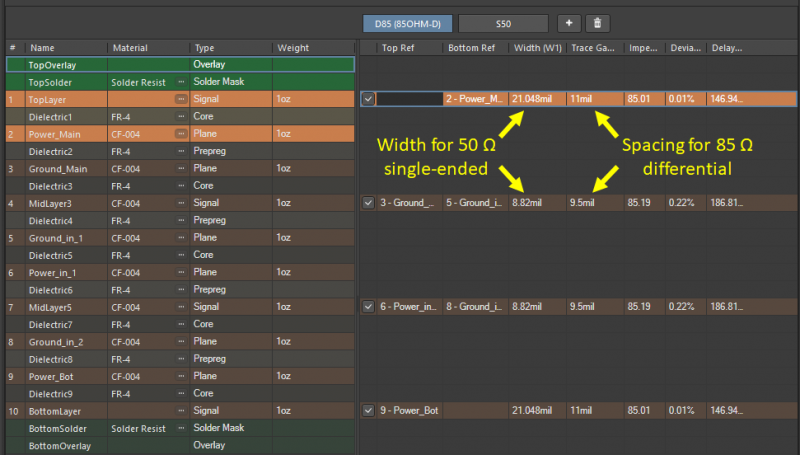
Altium Designer’s impedance calculator considers the entire high speed signal frequency range.
Consider High Speed Signal Frequency Range in PCB Stackup Design
The stackup used to build a real circuit board is a major determinant of signal integrity and power integrity. PCB stackup design will determine the trace geometry required for controlled impedance, but the impedance calculation needs to consider the entire signal bandwidth. This is because digital signals depend on frequency throughout their bandwidth, so there must be some way to account for variations in the dielectric constant of a PCB transmission line.
Just as the PCB stackup will determine signal integrity, it will also affect power integrity, particularly in high speed PCB designs. Again, the high speed signal frequency range extends across the PDN impedance in the PCB, so the PCB must be designed with adjacent power and ground planes to provide high interplane capacitance. Working with the best PCB stackup manager makes these tasks easy and helps ensure your next design will work as intended.
The Industry’s Best PCB Layer Stackup Design Utilities
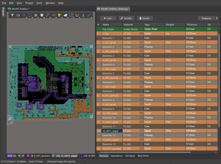
Altium Designer’s Layer Stack Manager is where you define your plane and signal layer arrangement to ensure impedance controlled routing, accurate propagation delay calculations, and laminate selection. Altium Designer’s PCB stackup design features are ideal for high speed circuit boards as they interface with an integrated field solver, giving highly accurate impedance calculations that include dispersion, copper roughness, and parasitics in transmission lines. While other PCB design platforms force you to use an external simulator for these tasks, Altium keeps you productive and ensures your calculations are accurate.
- The best PCB design software for interconnect design and routing will account for dispersion in your PCB substrate material and transmission line designs.
Learn more about dispersion in FR4 and how to account for it in impedance calculations.
- Your stackup affects many important aspects of power integrity and signal integrity, and it will be a major determinant of your product’s performance.
Learn more about the effects of PCB stackup design on high speed signals.
- The Layer Stack Manager in Altium Designer is where you design your board to have controlled impedance for specific laminates.
Learn more about the Layer Stack Manager in Altium Designer.

The Layer Stack Manager in Altium Designer gives you control over power integrity and signal integrity.
Access Routing and Simulation Tools for Your High Speed PCB Design
In addition to PCB stackup design features, high speed designs often require simulations to ensure the circuit board layout will function as intended. High speed PCBs also need the best routing tools to help ensure signal integrity in a new circuit board design. Once your design is routed and the layout is complete, simulation tools can be used to evaluate signal behavior and ensure the design will operate as intended.
Altium Designer gives access to both sets of features in a single program. With its integrated simulation engine, designers can use IBIS models for components and run simulations directly in their board layout, giving a complete picture of signal behavior. Routing can also be evaluated by simulating crosstalk and reflection waveforms in a design directly from PCB layout data.
Create Advanced Circuit Board Designs With Maximum Productivity
The rules-driven design engine in Altium Designer is ideal for high speed designs in advanced electronic systems. The circuit board design features in Altium Designer give you full control over every aspect of your design and help you prevent signal integrity problems in your finished PCBA. If you want to stay productive, look to Altium Designer to give you everything you need for your printed circuit board layout in a single application.
- When you need to account for signal bandwidth in your high speed designs, Altium Designer includes everything needed to design high-quality layouts and get them into manufacturing.
Learn more about Altium Designer’s unified design environment.
- The Layer Stackup Manager in Altium Designer includes an integrated electromagnetic field solver from Simberian, giving you ultra-accurate impedance calculations in your circuit board layout.
Learn more about the integrated field solver from Simberian in Altium Designer.
- When you’re ready to share your circuit board with other PCB designers or your manufacturer, Altium 365 lets you instantly share your design and production data through Altium Designer or on the web.
Learn more about sharing your PCB project data with Altium 365.

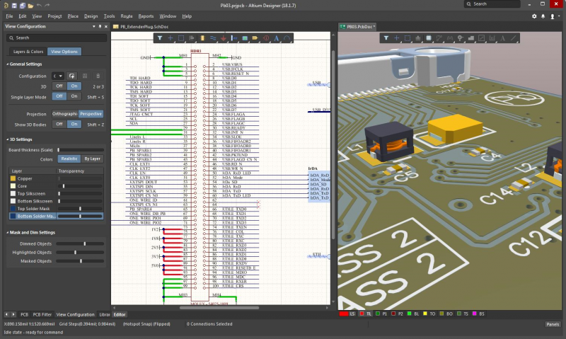
Use the complete set of layout tools in Altium Designer to create a high speed PCB layout.
Determining the important portion of a high speed signal’s frequency range doesn’t need to be a chore with Altium Designer. With its complete set of design tools in a single application, it’s never been easier to take full control over your advanced circuit board designs.
Altium Designer on Altium 365 delivers unprecedented integration to the electronics industry until now relegated to the world of software development, allowing designers to work from home and reach unprecedented levels of efficiency.
We have only scratched the surface of what is possible to do with Altium Designer on Altium 365. You can check theproduct page for a more in-depth feature description or one of theOn-Demand Webinars.
