Guidelines for Creating Useful Schematic Symbols
The schematic symbols that you use to represent the components are at the heart of your schematic design. The quality of the symbol and how it is arranged can be one of the most critical factors influencing your schematic’s readability. A poor quality schematic symbol will lead to an unreadable schematic sheet that is difficult to understand. I created the largest open-source library for Altium Designer over five years ago, initially as a way to clean up and re-organize my personal mess of library components. Since then, I’ve tried my best to figure out what makes a schematic symbol more readable and how it should be arranged to make everyone’s schematic clear and easily understood.
File Management
Before you even start working on the symbol, you generally need to think about file management. However, if you’re placing your components into Altium 365, this is taken care of for you by the platform. This thankfully means it’s not something you need to put any thought into.
If you’re not using Altium 365, you should think carefully about your folder structure and file usage for your SchLibs (and PcbLibs). It can be very convenient to dump all your schematic symbols into a single file. However, this makes version control a bit of a nightmare. Most version control systems cannot diff a schematic library file, making it very hard to track changes to a file. This is especially true if you use a distributed version control system, such as Git, that may have multiple users committing changes simultaneously.
For version control reasons, if not for your files’ tidiness, stick to just having one symbol per library file. I initially fought this idea but soon realized that it really makes life a lot easier after I switched. It also makes it far simpler to find which library file has which symbol or footprint within it! If you place the symbol name or footprint name in the file name, you can very easily find the right file to open. Instead of putting all my symbols in one big file, I group the individual files into folders as a way to make them manageable.
Standardized Symbols
If there is an industry-standard symbol for the part you’re creating, don’t reinvent the wheel. You can find a relatively comprehensive list of standard symbols listed on Wikipedia. Don’t overthink using standardized symbols; you don’t need to place them in a rectangle or do anything strange with colors. Just keep it simple using the standard Altium colors so your symbol blends in with any other symbols you might use.
Use the default grid; as a metric user, it’s so tempting to switch your schematics to use a metric grid size rather than the 100 mil default grid, but it’s just asking for trouble. If you mess with the grid when creating symbols, you will never be able to use symbols from other sources as they will not correctly line up with your components. Also, it’s very likely that you’ll be unable to make connections or find your schematic will get very messy at the very least, with lines not aligned to the grid.
Make sure all basic components keep to a standardized size and span. I make all my basic components have a span of precisely 400 mil (4 grid squares). This ensures I can line up resistors, capacitors, inductors, etc., as they will all have the same width and height.
Symbols for Integrated Circuits
Now we have reached the point where we need to talk about the real issue - how to make an integrated circuit symbol usable and conducive to producing readable schematics. Simply lining pins up around a rectangle to match the package pinout is a terrible idea. Package pinouts are not intended to create legible schematics; they are the arrangement that was most convenient for getting signals off the silicon die. They are what make the most electrical sense for the silicon inside the package. This means you can have ground and voltage supply pins intermingled with I/O pins. On a microcontroller, the chances are your port numbers will not be in numerical order on the package or even consistently placed between different packages with the same pin count.
Ideally, every Low Dropout (LDO) linear regulator symbol should essentially be a drop-in replacement for any other LDO in your schematic - regardless of the package or the pinout of the package. So, what rules and conventions can we put in place to make this happen?
I like to break the schematic symbol into six logical areas, the top/middle/bottom of the left-hand and right-hand sides. I do not place pins on the bottom or top to encourage signals to flow from left to right in the schematic.
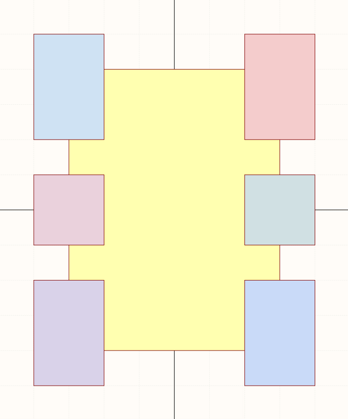
The top left-hand corner is dedicated to positive voltage inputs, no matter the type of IC. The bottom left is reserved for ground and negative potentials.
The Left-Hand Side
I see the left-hand side of the component symbol as the ideal place for what I like to call the administrative functions for most components. These are the pins necessary for the IC to operate, which have a fixed connection or signal that does not change while the circuit works. Some examples of such pins are:
- Power supply pins
- Reset/enable/under voltage lockout pins
- Clock/Oscillator pins
- Switch Mode setup pins (soft start, frequency set, compensation, synchronization)
- Soft start pins
- In-circuit programming pins if they are standalone
- Power decoupling pins for internal regulators
Try to keep pins that will be connected directly to ground at the very bottom and any pins that will connect to ground via a passive component just above them. This will reduce the clutter as much as possible and reduce the likelihood of nets wires needing to cross over each other.
Group power supply and ground pins together, with a single grid-gap between each different potential and domain (such as between analog and digital signals). When spacing out the other functions, consider how much of a gap you might need between them to add the components they will connect to. Oscillator pins are a great example of this, as placing them directly one on top of the other generally won’t leave much room for adding the crystal symbol along with its load capacitors.
The Right-Hand Side
On the right-hand side, we have the pins that will perform some action, carry a signal, or do something. I try to keep functions such as voltage regulator outputs or RF outputs in the top right-hand corner along with any related pins such as bootstrapping pins or switch pins and voltage feedback. Try to stack and space the pins so that you will be able to make connections to components with as few crossovers of net wires as possible. We’re trying to make the final schematic as clean as possible. If any components don’t have enough room or require connections that need to continually cross over each other, we won’t have a very readable schematic.
Try to maintain a standard order for common protocols. For example, for I2C, I always have SCL at the top, followed by SDA. This makes it quick and easy to read schematics once you know what standard the symbols will follow, as you know where to expect to find particular pins.
When dealing with microcontrollers or other logic devices, group by connections by port and place the pins in their port order. Try to include as full a description of the port as possible. Rather than using the label PIO0_22 for a pin, use the more informative “PIO0_22/AD6/CT16B1_MAT1/MISO1”. With this detailed description, we end up with a much bigger symbol. However, we can now quickly see that beyond being a general IO port, this port also supports ADC functionality, timer capture, and SPI1 MISO. With the full port description, we do not need to refer back to the data sheet to determine if a pin has any specific peripheral capability each time we want to wire up the microcontroller or move a signal to make routing easier.
When to Add Component Parts
Most EDA software allows you to break a symbol into multiple pieces. This is so you can place multiple symbols to define a single component. So, at what point should you use this functionality? Below are some suggestions.
Low Pin Count Components
While it’s evident that if a high pin count part that would be taller than a schematic sheet, then it needs to be split into multiple parts. However, there are often times when it also makes sense to break up a lower pin count component into parts. If the component has an array of identical functionality, such as a quad operational amplifier, breaking each amplifier into its own part can make a lot of sense. This can make your schematic sheet very clean as you can provide separation between each amplifier. In this case, I add the power supply pins to the first part, and the other parts are then simply the standard operational amplifier symbol.
Likewise, for motor controller ICs that can control multiple motors, you might have a part for the input power and those administrative functions that I mentioned earlier. This leaves one part for each motor that just needs to include its input and output pins.
Unless you have a component with an array of identical functionality that needs to be logically separated, as discussed here, you should try to keep a low pin count component as a single symbol.
High Pin Count Components
The most common use of component subparts is when a single component part will be simply too large to fit on a page. If you consider the size of the smallest standard page template, A4 or Letter, depending on your region, try not to let your symbol grow to larger than half the page height.
When splitting your microcontroller or other high pin count part up, consider where you put the break. For microcontrollers, try to keep the connections for a full port together, do not split a symbol halfway through a group of ports. This might mean that some symbols will be much smaller than others or that you end up with one sub-component per port on 32-bit microcontrollers that have 32 pins per port.
If your high pin count component has a lot of what I call administrative pins, such as power, oscillators, or static/fixed-function communication pins (like ethernet or USB), consider making a subpart for these functions and subparts for all the signal pins.
Think About Schematic Layout
Perhaps the most important thing to do when designing a schematic symbol is to look at the data sheet, consider drawings for typical applications and think how you could rearrange the vendor’s schematic to make it tidier. You can often find that moving a couple of pins around can significantly reduce the number of net wiring crossovers or the layout’s neatness. When designing your schematic symbol, put thought into how it will be connected and what supporting components will be required around it. Ensure all logically grouped pins are placed together and maintain consistency of where you place pins for similar component types. This allows them to be used interchangeably and means the reader of the schematic can immediately know where they should look to find a specific pin function.
Have more questions? Call an expert at Altium and discover how we can help you with your next PCB design