Ethernet Layout and Routing Standards: MAC, PHY, and RJ-45 Connectors

Ethernet over copper is likely part of the backbone of your office building’s networking infrastructure. Thankfully, Ethernet routing standards make it easy for designers to create everything from complex networking equipment to single-board computers for any application. The overall architecture for creating Ethernet-capable devices is deceptively simple, but certain rules should be followed to ensure signal integrity.
High-level Ethernet Layout, Routing, and Architecture
Within the IEEE 802 standards, Ethernet devices contain three primary elements, all of which must be routed together in a specific manner:
- Medium access control (MAC): The MAC is typically integrated into the processor of the device (FPGA, ASIC, MCU, or other component), or it may be present as a standalone controller. For high port count switches there are dedicated controller ICs for this function. The MAC provides control over determining destination addressing, sends along its own address to receive data, and duplexes and assembles data into packets for transmission to another device.
- Physical layer (PHY): The next stage in Ethernet layout routing is the PHY. This is typically an integrated circuit that converts the digital data from the MAC into analog signals for transmission down copper or optical fiber. Again, this could be integrated into the switch controller. If a switch controller only includes limited PHY space for a specific port count, the port count can be expanded with a dedicated PHY chip.
- Clock: The final important element is a clock that is used to trigger signal transmit and receive functions between the MAC and the PHY. In MII, a 2.5 MHz clock is used for 10 Mbps data rates, while a 25 MHz clock is used for 100 Mbps. In RMII, a 50 MHz clock is used for both data rates.
In the last point, I've only mentioned MII and RMII, but there are other MII standards that are used in Ethernet routing with that have similar requirements. However, these other standards, particularly GMII/RGMII, use 125 MHz clock. Take a look at this article to see more guidelines on the various MII standards.
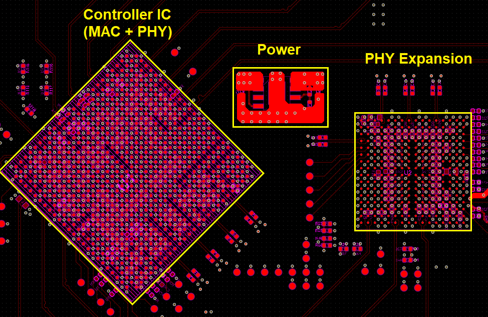
The image below shows an example portion of a layout for an Ethernet switch. This high port count switch uses a main controller ICM that includes the MAC and integrated PHY layer. This type of switch controller will typically support about 16 ports. The expansion PHY chip connects to one of the port outputs using an MII routing standard, and this chip provides the additional ports needed to increase the total port count of the switch. If you're using this system layout, pay attention to the required MII routing standard between the main controller and the expansion PHY.
If you're routing an Ethernet port to a processor, you generally won't have dedicated PHY chips or controllers. MCUs that support Ethernet (e.g., Microchip's PIC32 MCUs) will include an integrated MAC/PHY transceiver on the die, giving you a small footprint option. If you have an MCU that supports USB but not Ethernet, there are USB to Ethernet data converters that will let you route to an Ethernet port.
Ethernet PCB Routing
The standard routing protocols for Ethernet (MII and RMII) are compatible with 10Base-T and 100Base-TX, although similar routing standards are designed for 1 Gbps and higher data rates (GMII, RGMII, SGMII, QSGMII, I cover these in the article linked above). Routing uses 50/100 Ohm single/differential impedance, requiring impedance controlled routing over a ground plane. All routes within this scheme should be placed on a single layer with precise length matching. Next we need to consider routing between different chips in the system, and to the connectors.
Routing From the Controller IC/PHY
Normally, microstrips are used on the surface layer, but striplines can also be used. If you're designing a network switch with high port count, the controller ICs may have a BGA footprint, so you'll need an escape routing scheme. Normally dog bone fanout is fine; the pitch on these components is not super-fine and you'll be able to reach the first two rows of balls on the surface layer (see above).
Routing between the MAC and PHY follows either the MII or RMII routing standards with point-to-point topology. The primary difference between these two routing standards is the number of signals required to interface between the MAC and each PHY chip. In a multi-port device, two signals from the MAC can be shared among multiple PHY chips, while another 16 signals (MII routing) or 6-7 signals (RMII routing) are required per PHY chip. Obviously, the number of signals required to reach a large number of PHY chips quickly becomes unmanageable, thus RMII was developed to reduce the total number of signals by a factor of 2.
The output from the PHY (whether integrated in the processor, from a controller IC, or from a standalone expansion PHY) connects to an RJ-45 connector. These connectors require a specific termination scheme (see below) to preserve signal integrity.
With optical fiber networks, the output from the PHY connects to a separate fiber transmitter/receiver with its own layout rules. Commercially available transceivers are available with edge connectors or other connectors. This allows these transmitter/receiver modules to be swappable, ideally without taking apart an entire unit (e.g., hot-swappable interfaces).
Fiber optic media converter with an RJ-45 connector
Routing and Bob Smith Termination for RJ-45 Connectors
The routing requirements between the PHY chip and RJ-45 connectors are much more strict. TX and RX lines are routed as differential pairs, and these traces must be length matched and symmetric. Remember that this circuit and associated traces are carrying analog signals, thus they need to be routed over an analog ground plane. Make sure to design an appropriate mixed signal ground plane in your device.
There is also a specific termination circuit that must be placed between the PHY and the RJ-45 connector, commonly termed “magnetics” within the Ethernet layout routing standards. A magnetics termination circuit involves four transformers for a single RF-45 connector, two on each RX and TX differential pair.
One transformer is placed as a common mode choke, while the other is placed upstream (towards the PHY). Tapped ferritic transformers with 1:1 turns ratio are normally used to provide the required common mode noise rejection in the TX and RX differential pairs that connect the termination circuit to the PHY and RJ45. This also allows any required DC bias to pass to the termination circuit (e.g., to power any LED indicator lights in the connector).
Some application notes will recommend not placing a ground plane beneath the differential pairs. However, EMI susceptibility can be reduced by connecting common mode capacitors between the RX/TX traces and ground, in which case the analog ground plane should extend beneath these differential pairs. The differential pairs should be impedance matched throughout the termination circuits (called Bob Smith termination), and the common method is to include a Thevenin network or a pull up resistor near the PHY. In this case, a portion of the power plane will need to appear near the pull-up resistor.
Example industrial-grade magnetics termination circuit for an RJ-45 connector. Source: Renesas
Note that some RJ-45 connectors include this second transformer or both transformers as part of an integrated magnetics circuit. Always check the datasheets for integrated connectors to see what other components need to be added to complete the termination circuit. If these transformers and associated passives are not integrated, Ethernet transformer modules are also available as discrete components (usually in SMT packages). These discrete modules provide better ESD protection as there will be larger separation between each portion of the system.
A Note on Bob Smith Termination
There has been some debate as to whether Bob Smith termination is the best termination scheme for Ethernet. I've discussed this in a more recent article on my own site and here on Altium's PCB Design Blog. You can read the article here. If, for some reason, you don't want to use Bob Smith termination, be sure to test your channels thoroughly on a prototype to ensure your layout and routing will work as designed. Blindly following or ignoring standards doesn't guarantee your design will work, so be sure to test the design to ensure compliance with routing and EMI/EMC standards.
PCB Stackup for Ethernet-Capable Boards
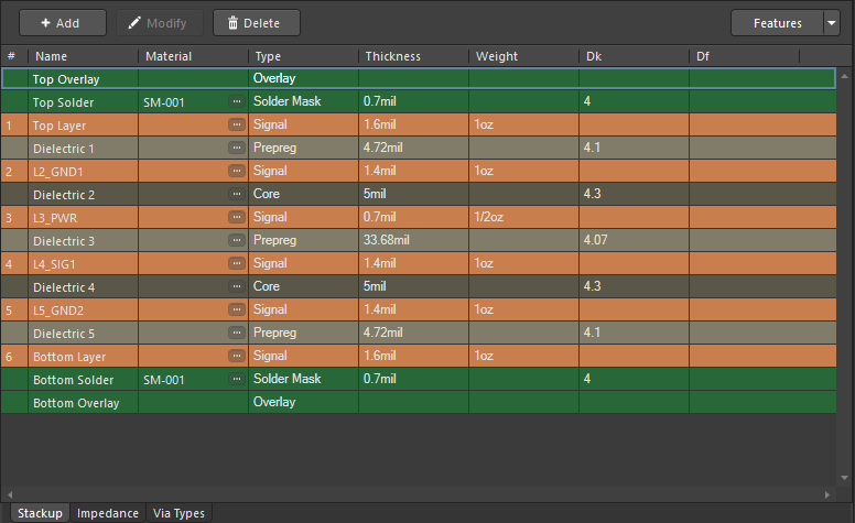
Finally, we can’t ignore the layer stack for Ethernet-capable PCBs. 2-layer or 4-layer stacks are generally used, although you could certainly use a higher layer count. In lower layer counts, power islands are generally used with a ground plane on the same layer. These planes should be decoupled with an appropriate capacitor. I haven't shown this explicitly, but the layout shown above does include a dedicated power regulator with caps placed near the controller and expansion PHY chips for decoupling.
The example below shows a 6-layer stackup that I've used for Ethernet switches. This PCB stackup can provide the required routing channels for accessing the inner balls on a controller IC with BGA footprint. This type of stackup will support at least 12 port switches without cramming signals into an excessively small space.
EMI in Ethernet Routing
Copper pour can also appear on the surface layer to provide extra shielding against EMI for critical circuits, which is may be desirable if your device will be deployed in an electrically noisy environment or if your design includes some other RF circuits. Be careful with this, however, as placing ground pour near the controlled impedance lines will alter their impedance. Make sure your routing tools include an integrated field solver that can ensure impedance profile conformance as you route your board.
Note that if you place ground pour on the surface layer, it should be connected to the lower ground layer, ideally with a periodic array of vias. Only place copper pour on the surface directly over a ground plane in the next layer. This is one strategy to deal with EMI/EMC compliance, but you don't need super-tight pitch if you are using a via fence to provide EMI suppression since you're only working at 100's of MHz.
When routing on the surface layer, you may need to route a signal over a ground plane and a power island for a single interconnect. This is generally a bad idea in any device as the portion of the trace that is not placed over a reference plane can radiate strongly, and the overall circuit it forms will have large loop inductance. To provide a return path and properly switch reference planes during routing, place a small capacitor (usually ~10 nF) between the ground plane and the power island that runs parallel to the trace.
More on Ethernet Routing, Layout, and System Design
If you still want to learn more about working with Ethernet, including modern gigabit Ethernet interfaces, read this excellent tutorial from Mark Harris. In that article, he gives a deeper dive into system-level design and the particulars of gigabit Ethernet, as well as some useful tips for layout and routing. Between these articles and some good reference designs from component manufacturers, you'll be well on your way to designing with Ethernet.
When you use a design platform like Altium Designer, you’ll have all the Ethernet layout and routing tools you need to design copper and fiber optic-capable networking devices. The schematic design, layout, routing, and many more features are all accessible within a single unified design interface. You’ll also have access to the industry’s best signal integrity and documentation features in a single program.
When you’ve finished your design, and you want to release files to your manufacturer, the Altium 365™ platform makes it easy to collaborate and share your projects. We have only scratched the surface of what is possible to do with Altium Designer on Altium 365. You can check the product page for a more in-depth feature description or one of the On-Demand Webinars.
Now you can download a free trial of Altium Designer to learn more about its full suite of design tools. Talk to an Altium expert today to learn more.
