Differential Pairs Without Ground: Is it a Problem?

Differential pairs have helped solve some basic signal integrity problems, and modern CAD tools make them easy to design and route. However, differential pairs are not the cure-all for every signal integrity problem, despite their usefulness in suppressing common-mode noise at a low-level receiver. There is one question that always gets asked when discussing differential pair routing: do these traces need a ground plane?
Sometimes, the answer to this question depends on who you ask and which conceptual example you use to explain how differential pairs work. Like most engineering questions that we encounter on this and other blogs, there are kernels of truth to all the answers you’ll find to this question, and it’s easy to take those points out of context. Let’s look at when you need to use a differential pair ground plane, and when it’s merely a bad idea to route differential pairs without ground.
What is a Ground Plane Anyways?
If you want to know when it’s appropriate to route differential pairs without ground, it pays to know what a ground plane does and why it’s important. First, let’s look at what a ground plane does physically (beyond just being a big copper conductor):
- Capacitance: When paired up with a ground plane on an adjacent layer, you’ve just created a physically large capacitor. When the two planes are close together (thin laminate between planes), you have larger interplane capacitance.
- Shielding: A ground plane provide a nice big source/sink of charge. How charge is drawn from or sunk into a ground plane is basically irrelevant. In addition, it provides image charge to terminate electrical fields pointing into the plane.
- Single reference point: Ideally, it provides a reference potential. In other words, it can be used to provide a reference point for any voltage measurement, including the voltage “measurements” used by ICs to force switching. The 3.3 V signal you measure at the driving end of a lossless interconnect is reasonably assured to be seen as 3.3 V at the receiving end.
Aside from some other features like providing a simple way to distribute heat and power throughout a board, ground planes provide some basic electrical functions that sometimes aren’t discussed until you get to a graduate level electromagnetism class. In any case, the last two points matter for differential pairs without ground. If you get your routing right, you might not need ground for differential pairs.
Your Differential Pairs, Ground Planes, and Signal Levels
The way in which a differential pair relies on a ground plane depends on a few factors and relates back to the parasitics that govern impedance. First, let’s look at the parasitics between differential pairs. All differential pairs have some small amount of parasitic capacitance between them, which combines with their parasitic inductance and the native parasitic capacitance with respect to the ground planes.
These parasitics produce two effects:
- The parasitic mutual capacitance and mutual inductance provide coupling between the two lines in the pair, which helps determine their differential impedance.
- The parasitic capacitance back to the reference planes allows a displacement current to propagate in the ground plane.
If there is a return current beneath traces in a differential pair (assuming we are speaking in the same way as we would for single-ended traces), it lies very close beneath the pair and is zero at the midpoint between the pair. For high speed signals, the distribution of any return current below the trace would be approximately Gaussian. This is shown in the graph in the image below.
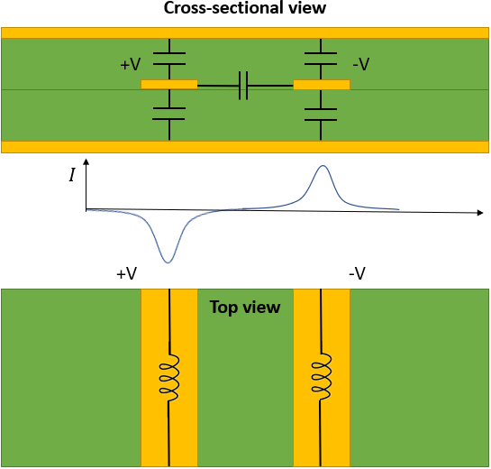
Here, to provide a “return path,” we don’t really need a ground plane. Imagine if we slowly increased the distance between the ground planes and the traces in the above figure. All electric field lines emanating from the positive trace would terminate at the negative trace. This explains the definition of differential impedance: it is the impedance between the two traces due to their mutual coupling. This also helps explain why signal levels in a differential pair are read as the difference between the values on each trace.
This is where someone will ask: “How does the current flow from the positive trace into the negative trace? It must happen through the IC!” Oddly enough, Lee Ritchey claims to know of a textbook that shows this specific graphic on the cover. Rather than asking where current flows, I suggest engineers get away from this idea that current “flows” anywhere like water in a pipe.
When a wave is excited at one end of the trace, the electric field is excited by some free charge distribution on the conductor. The electric field from one conductor induces polarization in the opposite conductor, which is seen as a displacement current. As the wave propagates down a differential pair, so does this charge imbalance along the two pairs. The rate at which this charge imbalance moves along the trace is indeed a return current. Note there is also a contribution from mutual inductance, and the same explanation applies.
Why Use a Ground Plane for Differential Pairs?
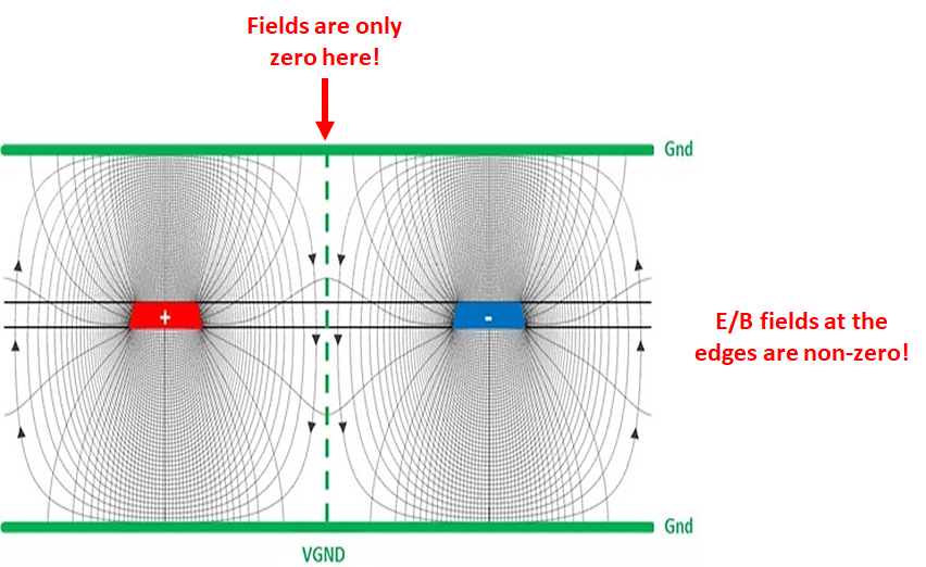
One point that everyone brings up with single-ended traces but forgets with differential traces is the level of isolation provided by a ground plane. Simply put, a ground plane near the differential pairs distorts the field lines and terminates them at the plane’s surface. If you have differential pair routing on two adjacent layers, you can isolate the pairs by simply putting a ground plane between the layers.
This leads to another reason to use a ground plane: suppressing differential crosstalk. The field lines shown below illustrate why differential pairs can induce crosstalk in a different trace, including in another differential pair. One either side of the trace. If you read the article I linked above, you’ll see that larger distances between a differential pair and its ground plane will increase the level of crosstalk induced in another trace (whether single-ended or differential).
This is due to the fields surrounding each trace in a differential pair, as shown in the image below. Here, the field is non-zero at the edges of a pair, meaning it can induce common-mode or differential noise in another trace. In addition to isolation between layers, using a ground plane also provides additional isolation between a differential pair and any other traces on the same layer. This might allow you to route traces closer together.
Note that, if you plan to use differential pairs without ground while preventing other EMI problems, you need to apply length matching so that the signals on a differential pair arrive at the receiver within their timing budget. This is because, when unmatched signals arrive at the receiver, their difference is measured, but any mismatch can produce a current pulse in the nearest ground region. If the ground region is far from the pairs (i.e., a far-away plane or the chassis), then you’ve created a short electromagnetic burst that can interfere with nearby components as radiated EMI.
Modern PCB design programs like Altium Designer® give you a complete set of routing tools for high speed impedance controlled designs, making differential pairs without ground an easy task. Altium Designer on Altium 365® delivers an unprecedented amount of integration to the electronics industry until now relegated to the world of software development, allowing designers to work from home and reach unprecedented levels of efficiency.
We have only scratched the surface of what is possible to do with Altium Designer on Altium 365. You can check the product page for a more in-depth feature description or one of the On-Demand Webinars.
