Designing Pressure Tolerant Electronics: It's All About Mechanics

After a recent inquiry from a customer about a high power board that must withstand high gas pressures, my team suddenly realized we needed to do some research on designing pressure tolerant electronics. This area is not as popular as designing electronics for ambient pressures, but the design techniques used here enable important scientific expeditions and industrial applications in high pressure environments.
Whether the board will be placed in a high pressure vessel or underwater, your design will need to withstand pressure to avoid failure. On the enclosure side, your vessel should be rated up to a certain pressure and may require frequent cycling to prevent implosion. On the electronics side, component selection and layout (especially at high voltage) become critical to preventing failure and ensuring reliability.
Sub-sea and High Pressure Atmospheres: The Design Approach
Prior to designing a pressure tolerant electronics system, particularly when there is no commercial-off-the-shelf (COTS) system on the market, designers should consider one of two approaches:
- Redesigning an existing system for ambient pressures to operate at higher pressures
- Designing a new system from scratch with existing or replacement components
Electronics designed for high pressure environments can be used at ambient pressure, but the converse is not always true. Taking an ambient product into a high pressure environment typically requires designing a pressure vessel with the appropriate pressure/depth rating. The term “pressure tolerant electronics” can also refer to a system designed to operate in a fluid-filled enclosure, which is intended to prevent implosion and reduce maintenance.
The enclosure for your electronics should be designed to meet a certain depth or pressure requirement for your application, which is a specialized area of mechanical design. The interior of the enclosure can still be brought up to a high pressure using air or an inert gas, which reduces the pressure gradient on the enclosure at the desired depth.
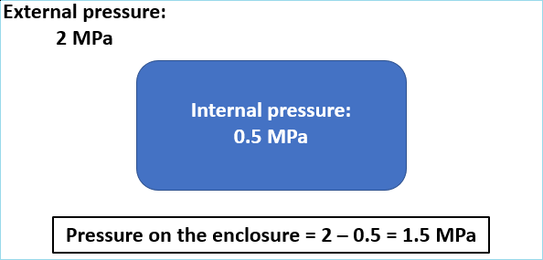
Successful design of pressure tolerant electronics requires elements of mechanical design in two areas: enclosure design and component selection. In high-pressure applications such as for an instrument placed in an atmospheric chamber, the board will usually be subjected to uniform stress and will compress evenly. The challenge is to build the enclosure to withstand high pressures and prevent implosion (or explosion for an internal high pressure atmosphere).
Component Selection for Pressure Tolerant Electronics
Perhaps the most important point, aside from the mechanical characteristics of a pressure tolerant board, is the selection of components. Perhaps the most well-known engineer working in this area is Nic Bingham, Lead EE of the Schmidt Ocean Institute. His research on electronic component selection and behavior in high pressure environments is extensive and spans integrated circuits, passives, motors, LEDs, and much more.
Components can also become compressed at high pressure, so components should be chosen judiciously. Without repeating all of Nic’s remarks on component selection, I’ll summarize the important points about selection of ICs and passives, as these comprise most components you’ll work with.
Passive Components
Some of the most important passives, which component selection tips for pressure tolerant electronics, relate to the internal structure of various passives.
- Resistors: Carbon film is normally porous and its resistance will decrease as pressure increases. However, most thick and thin film surface-mount resistors are also void-free, and will exhibit small resistance variations at high pressure. Thin film metal resistors are preferable.
- Capacitors: Polymer film capacitors are preferable, followed by ceramic and electrolytic capacitors. This is due to the high compressive strength of ceramics.
- Inductors and transformers: Shielded and unshielded ferrite core inductors and transformers are known to exhibit small variations in ferromagnetic behavior at high pressure.
Integrated Circuits
Conventional epoxy-packaged ICs exhibit similar deformation as FR4 and other resin impregnated laminates, so the pressure-induced forces on solder joints are small. The reliability of BGA components is still an open question. In terms of reliability, bond wires are at risk of fracture at very high pressure due to shrinkage of the die in integrated circuits. It’s not that the die is compressed, the problem is that it can be compressed to a greater extent than the package.
High Voltage and High Pressure
So far, we’ve focused on the mechanical design and component selection, but one important electrical aspect of pressure tolerant electronics concerns the breakdown field of air or other fluids/gases at high pressure. When high voltage exists between two conductors in a board, an electrostatic discharge and dielectric breakdown can occur when the conductors are close together. This is one of the primary reasons for the IPC 2221 standards on high voltage boards.
When a board is placed in a high pressure atmosphere, the breakdown field increases approximately linearly, following a trend known as Paschen’s law. This allows high voltage pressure tolerant electronics to be designed with smaller spacing between components while still complying with important industry standards.
The ECAD/MCAD collaboration features in Altium Designer® are unmatched by those found in other EDA applications. When you use Altium Designer, you’ll have access to a complete toolset for designing pressure tolerant electronics, and much more. All these features are accessible in a single design environment, which helps you remain productive and get to market quickly.
Now you can download a free trial of Altium Designer and learn more about the industry’s best layout, simulation, and production planning tools. Talk to an Altium expert today to learn more.
