Design Your Own USB-MicroSD Card Reader PCB
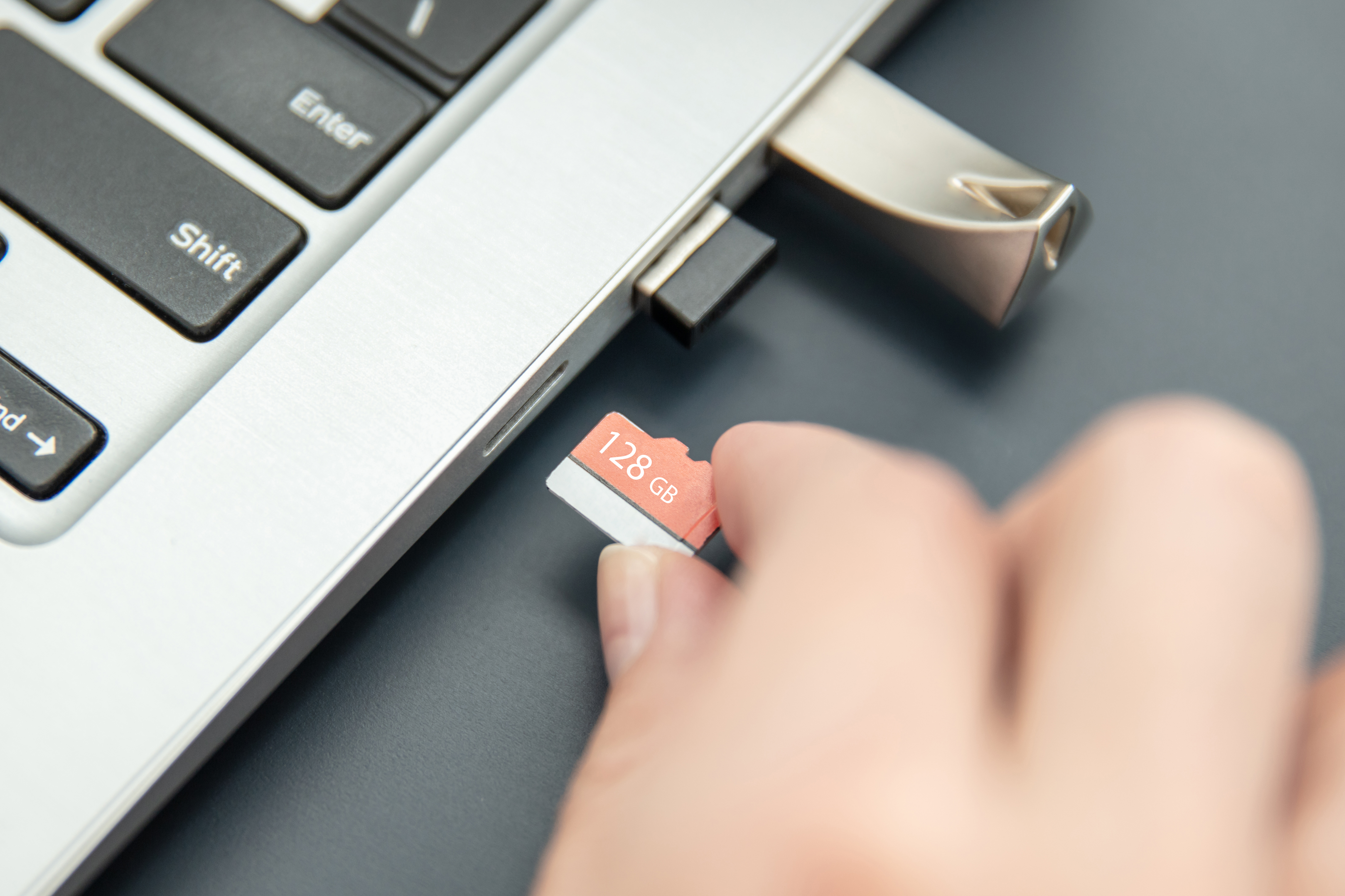
I’ll be honest, I still use an MP3 player with a 32 GB microSD card. I go running most days, and the last thing I need is to drop my phone in the street and watch the screen shatter, thus the $30 MP3 player. This also means that I need a USB-microSD card reader in order to switch out music on my memory card.
These cards aren’t limited to use in MP3 players, they also provide add-on memory for single-board computers like the Raspberry Pi. Ironically, you won’t find adapters for these cards in many laptops, you’ll have to swap cards in your phone and use your USB port to access data, all while funneling data between your cards and your computer memory. In this post, I’ll show how you can design a simple USB-MicroSD card reader for easy data transfer between multiple microSD cards.
Our USB-MicroSD Card Reader
If you plan to follow along with this project, you’ll need to create a blank project in Altium Designer® to get started. I’ll name this project “USB to MicroSD.PrjPcb” and add a blank schematic.
Schematic
This project isn’t too complex and all the required components can fit into one schematic if the sheet is large enough. You can see the schematic for this card reader below.
.png)
Some notable components in the schematic include:
- U1: AU9331 USB Digital Card reader IC
- U2: PRTR5V0U2X ESD protection diode
- U7: LM1117MPX-3.3/NOPB to get 3.3 V supply voltage from USB power.
- U8: I2C Serial EEPROM (FT24C08A-USR-T)
- J1: USB Type-A female connector
- J5: MicroSD connector
The easiest way to access these components is to use the Manufacturer Part Search panel in Altium Designer®.
To keep the design from getting too messy, I’ve used net labels on multiple nets. In this design, we have both single-ended nets and differential nets for the USB signals. Therefore, we need to properly name the differential nets with suffixes “_P” and “_N” to define positive and negative ends of a differential pair net, respectively; you can just follow the connection name in the schematic symbol for J1. Next, we need to place a differential pair directives on each net in the pair. I’ve done this with a blanket directive (see Figure 2 below).
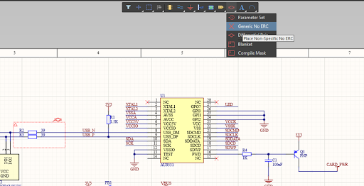
Finally, there are some unused pins on U1 in the finished schematic. To prevent ERC errors, we need to mark those pins as No ERC. Click the right mouse button and select “Generic No ERC” or press ‘P’+’V’+’N’ on the keyboard. You can then click on the unused pins to suppress any errors in the schematic.

Aside from these two points, the rest of the pins in the schematic can be wired as shown in Figure 1 without much more work. Be sure to place net names as shown above as this will make the schematic much easier to see visually. At this point, we can start working on the PCB layout.
PCB Layout
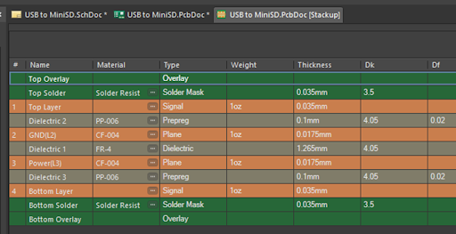
Before getting started on a new layout, it’s best to define your layer stack, create any required impedance profiles, and set up your design rules. The first two points can be done together in the Layer Stack Manager. We need to match 90 Ohm differential impedance/50 Ohm single-ended impedance for the USB data lines. USB differential signals will be placed on the top layer and will reference layer Layer 2 (GND plane). If you want to see how you can do this process, take a look at this blog, where I’ve gone through this process. Figure 4 below shows the stackup used in this board.
If you look through the blog I linked above, you’ll also see how to set routing rules for the USB differential pairs. This feature in Altium Designer ensures your impedance stays within your design constraints. All the design rules you need to modify can be accessed in the PCB Rules and Constraints dialog (open the Design → Rules menu). Here, the two important constraints you’ll need to modify are:
- Electrical → Clearance
- Routing → Differential Pairs Routing
Layout and Routing
Once the design rules are set up, you can import the schematic data into your new PCB layout and start arranging components. Here, we don’t have any particular form factor we’re targeting, so you can set up a board size that works for you. If you find the board size is too large or small, you can always change it later.
Once your components are imported, it’s time to start routing connections between components. Click the icon to interactively route connections or press ‘Ctrl + W’ keyboard (Note: Whichever layer is active, the trace will begin on that layer). I won’t show routing for every trace as the process for this board is rather straightforward. However, there is one useful routing feature I’ll use to route through a couple tight spaces in the layout.
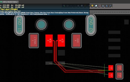
If you look below, you’ll see there is a spot where the USB differential pairs will not fit through a gap, either forcing components to be moved or forcing an odd route to the destination. This frustration is even more likely during differential pair routing because the pairs take up space. You can use the visualize clearance boundaries feature to see the no-go clearance area defined by the existing objects + the applicable clearance rule. Press Ctrl+W to toggle the feature on and off while routing.
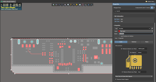
Once you remove all unconnected nets (except PWRpower signals), we can connect them with a polygon pour. Select Place/Polygon Pour or press ‘P + G’ and draw the GND polygon region. Double click the polygon to open the properties window, set the net name of the polygon to GND, and check ‘Remove Dead Copper’. Finally, do the same for the power polygon on the power layer. Then you can see all unconnected rats nest wires are removed.
Once you’re finished with the layout, it’s a good idea to run a DRC to check any design rules that were not enabled during layout and routing. At this point, you can use the manufacturing preparation features in Altium Designer to get your board ready for fabrication and assembly. You could even use Altium 365® to share your PCB project files and output files with your manufacturer.
We have only scratched the surface of what is possible to do with Altium Designer on Altium 365. You can check the product page for a more in-depth feature description or one of the On-Demand Webinars.