DDR5 vs. DDR6: Here's What to Expect in RAM Modules

If you read through most digital electronics textbooks, they still talk about fanouts and propagation delay within integrated circuits. Most textbooks still discuss digital electronics in terms of rise/fall times of 10’s of ns. Modern digital systems throw the textbooks out the window, and high-speed DDR memories are a perfect example of the paradigm shift that occurs when you jump into IC and PCB design. With DDR5 still being finalized, and DDR6 now being discussed, designers who are already comfortable with DDR4 will need to consider how their design practices should adjust to accommodate the constant doubling of data speeds in these high-speed memory technologies.
Signal integrity at the interconnect level, in terms of channel losses and impedance matching, was the primary concern up to DDR3. Once you hit DDR4 and higher, problems like dispersion, jitter, and copper roughness start to eat up bandwidth and your bits. DDR5 changes the game again with equalization for single-ended nets to compensate for dispersion and reflection-dominant losses. So what can designers expect from DDR6? Let’s look at a comparison of these two technologies as a comparison will help the avid computer peripherals designer prepare to use both.
From DDR1 to DDR5 and Beyond
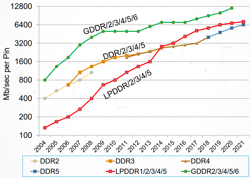
The introduction of DDR was arguably when the electronics industry moved into high-speed digital. Certainly, ECL logic components played a role, but DDR memories have been a prime example revealing steadily increasing data rates over time. The JEDEC standard for DDR5 is still being finalized (and has been since September, 2019), but the industry is already looking ahead to DDR6. This makes me think of the fundamental role applied researchers play in telecom, where engineers are already developing for 6G before 5G rollouts have even completed.
Up to DDR3, designers needed to be worried about designing to accommodate setup and hold times and controlled impedance on buses. Dispersion compensation was not such an issue up to the high end of DDR3 data rates as jitter started to become the primary problem in signal interpretation. Relatively small jitter that would be seen in low-level signals would be large enough to close an eye diagram for DDR3 signals. Thus the JEDEC standards were updated to provide design tolerances on eye diagrams for DDR4.
DDR5 Goes Faster, Not Wider
DDR5 takes the top-end DDR4 data rate and doubles it again by making buses faster, rather than wider. You’re still dealing with DDR4 routing challenges in terms of laying out parallel single-ended nets, but these channels are much shorter. Buses will also run fast enough that bit errors are dominated by reflection losses at the receiver, at any layer transitions, and due to dispersion. Shorter channels effectively reduce the total insertion loss but return loss dispersion needs to be compensated with extremely accurate interconnect impedance design out to high bandwidths.
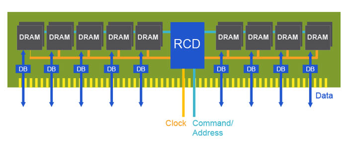
For DDR5, data transfer occurs in short bursts on single-ended nets with bidirectional communication. A full-speed clock allows switching between reading and writing at each end of an interconnect. Everything must switch extremely quickly, which required impeccable PDN design to suppress jitter as much as possible. PDN impedance on a typical circuit board can only get so low, and the low signal level in DDR5 (1.1 V max) puts very tight ripple/jitter limits on digital signals. These problems with reflection dominated channels and low ripple requirements superimposed on low-level signals have now forced the use of equalization in controllers for DDR5 interfaces to compensate for signal distortion and intersymbol interference (ISI). Note that this equalization is already used in high-speed differential serial standards (e.g., LVDS in SerDes channels).
There are plenty of other design challenges to consider in DDR5, but those listed above are arguably the greatest. You can read more about DDR5 PCB design challenges in an earlier article.
What about DDR6?
Just like earlier generations, DDR6 intends to provide up to double the maximum data rates in DDR5. If you’re innovating modules for DDR6, there are still plenty of unanswered questions. It’s generally agreed that buses won’t go wider, and speeds in DDR5 are already fast enough to hit the so-called “memory wall.” This leaves modulation (such as PAM or QAM) as the last available option to increase data rates beyond fully analog channels (e.g., 100G Ethernet).
Since going to an analog, high-speed channel undoes everything we know about DDR, and you’ll likely see PAM or QAM coupled with some proprietary equalization schemes embedded in controllers. Although the primary challenges lie with IC designers, board designers still have plenty to contend with when we look at the high bandwidth signals used in DDR6 channels.
PCB Design Challenges in DDR5 vs. DDR6
The challenges in DDR6 occur largely at the chip level, but the same board-level challenges in DDR5 also apply to DDR6. The power integrity challenge in DDR5 I mentioned above isn’t going to go away in DDR6. The power integrity challenge with DDR6 is extending flat PDN impedance out to higher signal bandwidths once modulation is imposed on DDR6 signals. Extending flat PDN impedance out to higher frequencies is all about keeping jitter at the Tx side low, which then keeps ISI at the Rx side low enough so that signals can be resolved with equalization. On-board power management ICs for DDR5 modules will probably also appear on DDR6 modules to help regulate power throughout the module.
Embedded systems designers will likely be on the tail end of DDR5/6 users. They’ll have an easier time than systems that use modules (PCs and servers) as losses at connectors are eliminated and are moved off to the ball/die level. However, the smaller space is a double-edged sword for the embedded designer. These systems are smaller, so they already expect to mount memory ICs on the board close to the system controller. However, they now have a more difficult time with radiated EMI between board sections due to the smaller space.
Something as simple as shielding between different functional blocks is useful, both for embedded and PCs/servers. Here, we’re talking about around two possible types of shielding:
- High bandwidth isolation structures. These structures can be tuned to provide high isolation up to high frequencies. They take up space on the surface layer, but these structures become smaller than when tuned to higher frequencies. This is an option for embedded systems, where the RAM ICs are placed on the same board as the controller.
- Creative routing on different layers. You can take advantage of internal planes to prevent crosstalk between different DDR buses on the motherboard. Once you break through the connector to the module, the modules are likely to be far enough away from other circuits that crosstalk is no longer a problem.
When new technologies like DDR5 vs. DDR6 come along, you need the design features in Altium Designer® if you want to lead technology development. Altium Designer includes a set of powerful layout and routing features that are ideal for high-speed applications.
Altium Designer on Altium 365 delivers an unprecedented amount of integration to the electronics industry until now relegated to the world of software development, allowing designers to work from home and reach unprecedented levels of efficiency.
We have only scratched the surface of what is possible to do with Altium Designer on Altium 365. You can check the product page for a more in-depth feature description or one of the On-Demand Webinars.
