Antenna Impedance Matching Network Simulation in Altium Designer
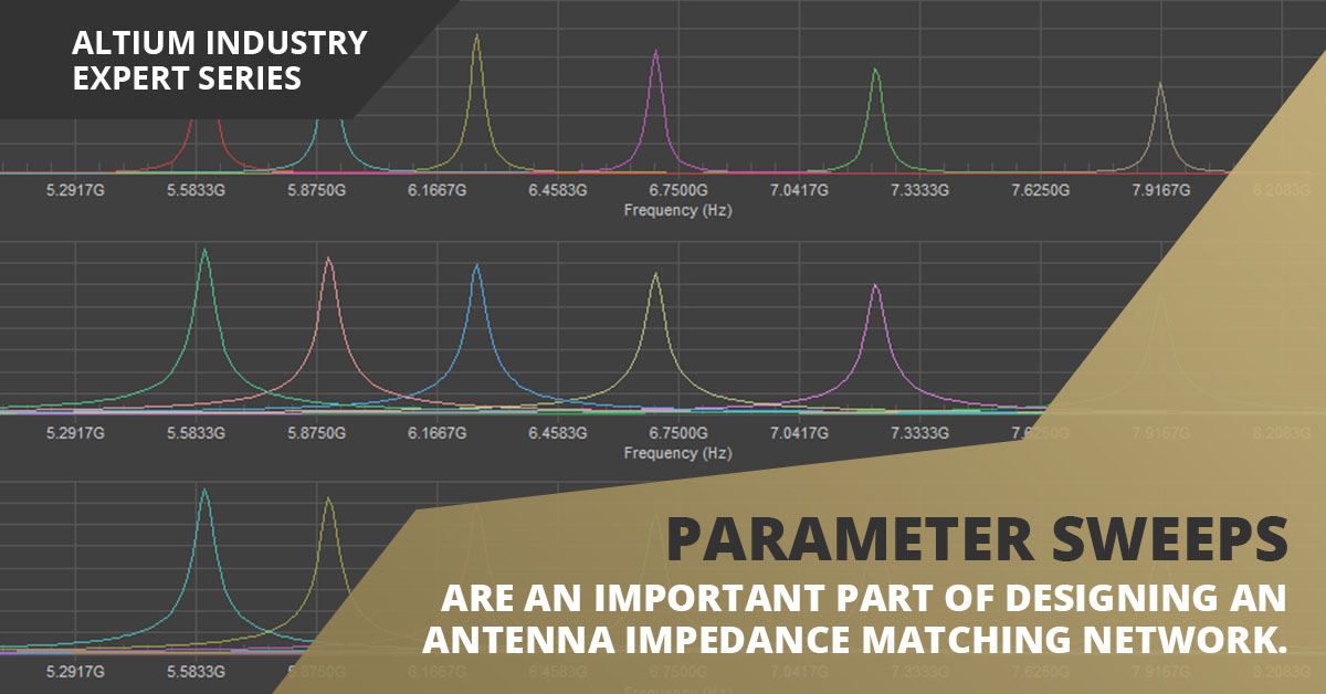
Just like driver and receiver components connected to transmission lines, antennas need to be impedance matched to their feed lines. Some common matching schemes that also provide filtration are built as LC networks, where capacitors and inductors are placed as series and shunt elements in the antenna impedance matching network. With multi-band antennas, wideband antennas, or extremely narrow-band antennas, these networks can get quite complicated. This is where a set of powerful simulation tools which enable parameter sweeps and frequency sweeps becomes important for designing antenna performance.
With the set of SPICE simulation tools in Altium Designer, you can design and match your impedance matching network in your schematic and simulate its behavior. In this article, I’ll show some simple steps for designing and simulating common matching networks for ~1 GHz frequencies and analyzing the results.
Building an Antenna Impedance Matching Network
The easiest way to design an impedance matching network is to construct a bandpass LC filter and take the voltage across one of the elements as the voltage seen by the antenna. The antenna impedance should generally be known, and your goal is to carefully tailor the transfer function for your antenna impedance matching network to the operating frequency of the antenna. The problem with this approach is that you normally have to set the operating frequency at the edge of the filter’s bandwidth, which makes the antenna sensitive to undesired frequencies. With this simple network, some external filtration circuit is typically required to remove any undesired frequencies.
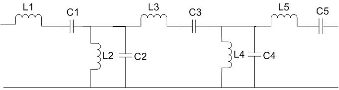
A better option is to design one of the common antenna impedance matching networks; the most common are the L-network, T-network, and Pi-network. These networks are basic LC networks with two elements. The basic layout for a wideband antenna impedance matching network is shown below. In this circuit layout, you are essentially combining bandpass and bandstop networks in series at successively higher frequencies, which then combine to create a transfer function with a flat band at the output. This type of impedance matching network is solvable by hand in principle, but working with a set of simulation tools can help you save time when designing this type of antenna impedance matching network. The image below is just one of many variations for pulling up or pulling down the impedance of an antenna such that it matches the impedance of the feed line.
The key points to consider when designing an antenna impedance matching network are as follows:
- Impedance and power at the desired frequency: Your design goal is to maximize power output for a given input signal amplitude at the desired frequency while ensuring the equivalent impedance of the network matches the impedance of the antenna.
- Bandwidth: If you are only working at a single frequency, a very narrow range of frequencies, or a modulated signal, then you need to check that the impedance and power output from the network are as flat as possible within the desired bandwidth.
A Bandpass Antenna Impedance Matching Network Simulation
In a simulation, you want to tune the impedance of the matching network such that the impedance of the network in parallel with the antenna impedance produces an equivalent impedance that matches the impedance of the feedline. In other words, your goal is to check that the voltage drop across the matching network plus the load impedance is equal to the desired impedance value.
In the forthcoming simulation, I want to match a 50 Ohm driver to a 70 Ohm antenna, so the impedance of my matching network plus the load needs to be 50 Ohms. The image below shows a schematic of my impedance matching network. Here, my simulation source is a simple AC source (labelled V2, found in the Simulation Sources.IntLib library). I’ve used a generic resistor to set the driver impedance to 50 Ohms, and I’ve placed a few probes for measurements. In this simulation, I have a proposed design for a matching network, and I want to see the bandwidth, impedance, and sensitivity to changes in some component values. Note that, in this simulation, the antenna must be modeled as a resistor.
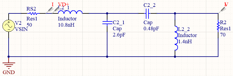
If you don’t have a simulation model for a specific antenna, you can use a resistor or other input network to simulate the load resistance/impedance. Note that this will not account for the modal distribution of a real antenna, but it is perfectly acceptable for designing an antenna impedance matching network.
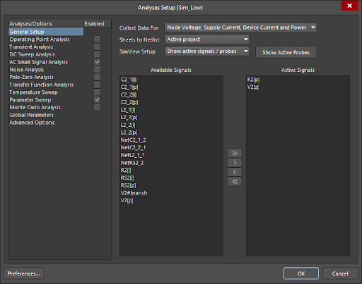
Here, the antenna would appear connected to the same point as the V probe. Note that you could place probes anywhere you like and calculate the network impedance manually, although the best way is to use the SPICE simulator to calculate it directly. To do this, create a MixedSim profile and enable the following analyses:
- AC Small Signal Analysis: I’m going to sweep the frequency of V2 from 100 MHz to 3 GHz.
- Parameter Sweep: I’m going to sweep the value of inductor L2 from 1 to 2 nH in steps of 0.2 nH. Note that you could sweep any of the components you like in this simulation.
- v2[z] (impedance calculation) and r2[p] (power calculation): In the window below, I’ve enabled v2[z] as the active signal, which will show the impedance spectrum of the entire network. The r2[p] signal will show the power dissipated across the load.
The results below show the parameter sweep and AC sweep results. As the inductance of L2 increases, the primary function is to increase the power dissipated across the resistor R2. This makes sense as the two elements are in parallel. From this set of plots, we can see that the maximum power dissipation across the load occurs at approximately 1100 MHz.
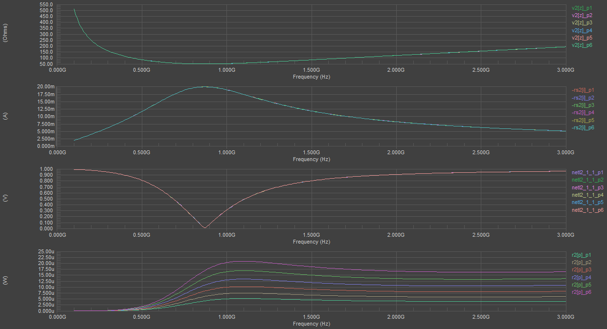
Note that the impedance spectrum shown above is the total impedance of the input resistance (RS2) and the impedance of the matching network/load resistor combination, which is a complex function of frequency. To see the real and imaginary parts, you simply need to create a new plot in the above window. Right-click on the impedance plot, and click “Add Wave to Plot”. Scroll through the list of waveforms and find the v2[z] entry. If you click on this, and then select “Real” on the right hand side of the window, you’ll add the real part of the circuit’s impedance to the graph. Use the same procedure to add the imaginary part of v2[z] (reactance) to this plot. My impedance spectrum for the as-designed schematic (i.e., without the parameter sweep) is shown below. You could also use this same procedure to get the real and imaginary parts of the voltage and current measurements.
To get the impedance spectrum of the matching network + the load, simply create a new plot with a custom expression: take the voltage across the network (netl2_1_1 waveform) and divide it by the current flowing into the network (rs2[i] waveform). You can produce three curves with the real part, imaginary part, and magnitude of the network + load impedance.
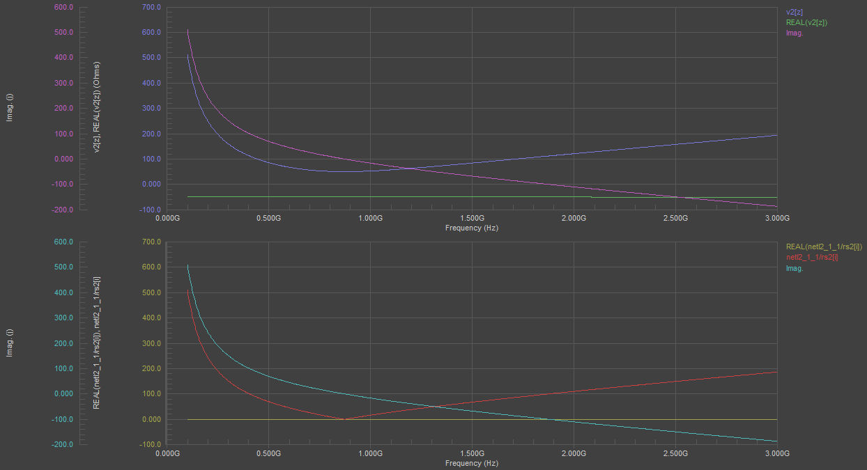
There are a few ways to interpret the above results. First, the impedance matching network functions as a filter with a resonance frequency of ~872 MHz; this can be seen in the plot showing the voltage drop across RS2. Second, the network impedance + load is 50 Ohms at ~1311 MHz. This can be seen by reading off impedance values in the bottom plot. Similarly, the v2[z] plot shows the total impedance seen by the source; the total impedance is 100 Ohms at ~1311 MHz (50 Ohms from RS2, and 50 Ohms from the network + load resistor), with the load resistor dissipating ~0.1 mW of power at this frequency. Note that there is another frequency for perfect matching, which is ~570 MHz. However, at this frequency the impedance of the matching network will dissipate the majority of reactive power, and the load resistor only dissipates ~1600 nW at this frequency.
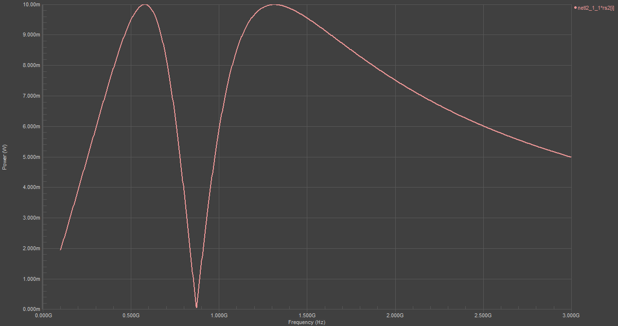
To see this more clearly and to see the power dissipation across the entire network, create a plot showing the magnitude of the voltage multiplied by the current across the entire network. The expression for this waveform is: netl2_1_1*rs2[i]. The image below shows a plot with the power dissipation across the combined matching network + load resistor. Note that this is effectively a dual-band matching network, but it functions poorly at the lower frequency band.
Since most RF folks prefer working with S-parameters, I’ll look at taking similar results and converting them to S-parameters in an upcoming article.
Once you’ve determined the approximate component values you should use for your matching network, you can then look through the manufacturer’s search panel to find real components that come close to the desired component values. After adding these to a real schematic, you should simulate this circuit again with COTS components to ensure your design will work as intended.
The pre-layout simulation features in Altium Designer® give you access to more than antenna impedance matching network design. These tools help you run a number of other important signal integrity analyses directly from your schematic. You’ll also have the tools you need to import your data into a new layout and begin designing your PCB.
Now you can download a free trial of Altium Designer and learn more about the industry’s best layout, simulation, and production planning tools. Talk to an Altium expert today to learn more.
