3D Printing PCBs and Generating Printing Models
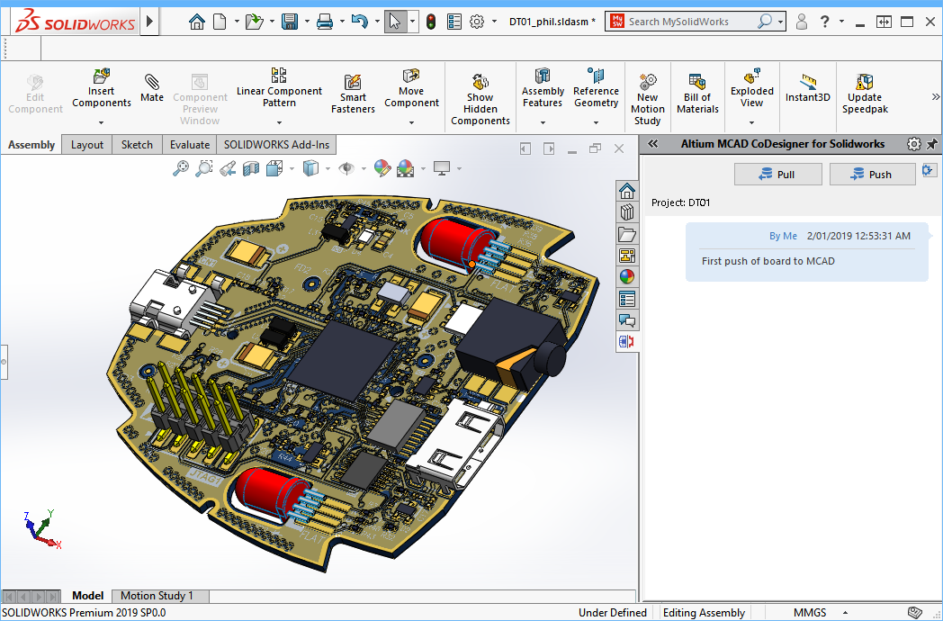
I’ve been enjoying working with Altium Concord Pro® hosted on the Altium 365® cloud recently. One of Altium 365’s best features is the support for mechanical collaboration with SolidWorks, PTC Creo and Autodesk Inventor. Thanks to the project hosting features through Altium 365, it's easy to open a shared project in Altium Designer and import it into one of these popular MCAD applications.
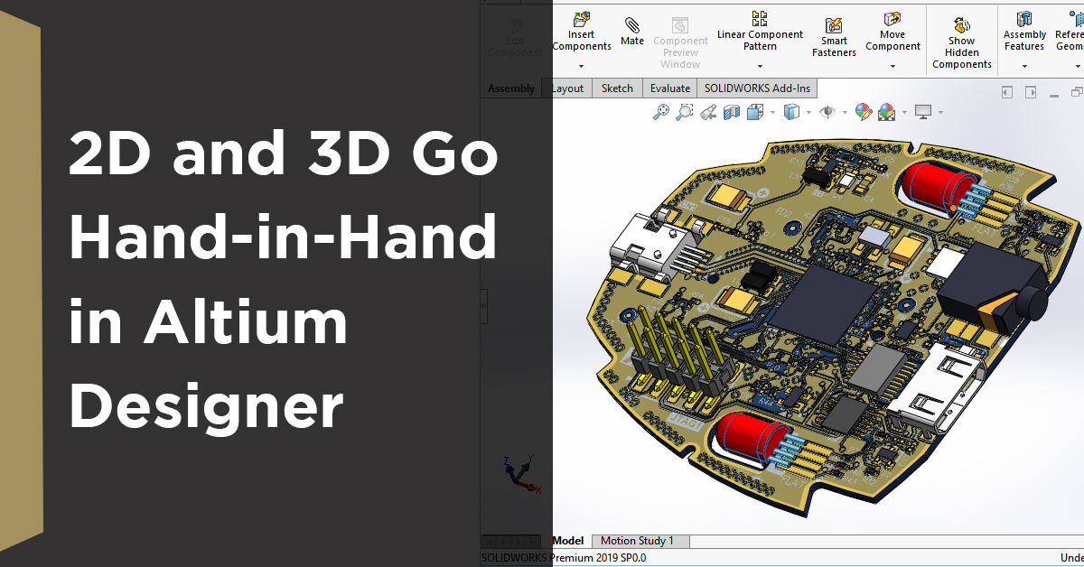
Altium Designer® was the first software in the ECAD industry to embrace 3D seriously. Most ECAD software has always integrated some sort of 3D export, but in my personal view, the features were often half-hearted attempts meant at most to check if the board fit the enclosure. Altium Designer offers a fully integrated environment where 2D and 3D go hand-in-hand, and you can do 2D layout functions in the 3D MCAD view in Altium Designer. The 3D-first approach has always been one of the platform strongpoints and is one of the many reasons I always ended picking Altium Designer as my go-to ECAD software.
The feature has been an absolute life-saver on multiple occasions when working in the power inverter industry. Power inverters have bulky electrolytic capacitors, PFC coils that dissipate considerable amounts of power, and power modules whose pins barely allow you to meet isolation requirements. All these components often need to be fitted in close proximity to capacitors the size of a can of Coke.
The MCAD Altium CoDesigner extension is bundled with every Concord Pro on Altium 365 account, and it enables seamless integration and collaboration between mechanical and electronic engineering. The process of designing power electronics is intrinsically three dimensional; physics doesn’t care about our love for fitting the universe onto flat sheets of paper. The sophisticated heat and charge transfer patterns of power appliances need to be modelled, analysed and understood in 3D to enable a competitive time-to-market and a compact form-factor. Altium Designer allows me to do that during every second of the design process.
What About 3D Printing PCBs?
Still, there is a piece of the puzzle that doesn’t fit. I would love to have physical 3D prototypes of my boards at the same time mechanical prototypes of the enclosures are printing in my 3D printer. If you want to 3D print PCBs or enclosures for your PCBs, you need to generate printing instructions for your design, either with a standard MCAD application or a mesh file generator.
Many have tried to convert the STEP 3D outputs of Altium Designer into standard formats for the 3D printing industry, such as STL or OBJ, with mixed results. The resulting files are often very heavy and prone to errors when imported into 3D printing software. Some 3D printer companies have software that can convert your design into one of these formats or a proprietary format, but these outputs are designed for specific 3D printers rather than being universal outputs.
Some components often disappear altogether, and I can testify it seems to happen more often with connectors, perhaps the most critical component in mechanical integration. The issue persists when going through 3D CAD such as Solidworks or PTC Creo. In this article, you can find out why it happens and how to address it. Spoiler alert: it’s not Altium’s fault.
What is a Mesh File?
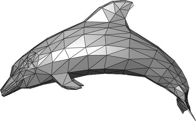
A mesh file, or more precisely a polygon mesh file, contains vertices, edges and faces that together define the shape of a 3D object. The goal in creating a mesh file is to rebuild the 3D object with these polygons so that we approximate the true shape as a combination of polygons.

In mathematical terms, the resulting object is a very weird polyhedron, most commonly composed of an enormous number of triangles with overlapping vertices. Triangles are most commonly used to represent complex 3D structures because they can very nicely approximate curves, whereas cubes or parallelepipeds leave jagged edges along a curved surface.
Mesh File Formats
The most common mesh file formats used in 3D printing are STL, OBJ, AMF and 3MF.
- STL is the de-facto standard for modern affordable 3D printers. It supports only the most basic geometry information, but it cannot encode colour or additional metadata. The format dates back to the first commercial 3D printer in 1987, the SLA-1. The industry has long settled on STL as a standard, but the format is prone to errors, and the resulting files can be heavy and slow to read.
- OBJ is a more modern alternative that allows colour data to be stored, and it supports more advanced surfaces than the triangular meshes of STL and is used mostly with colour 3D printers.
- AMF was introduced as the ASTM standard file format for 3D printing in 2011 and was meant to be an alternative to the STL standard format.
- 3MF has overtaken AMF in recent years, which is open source and supported by numerous 3D printer manufacturers and software houses.
Altium Designer can export 3D board data in either STEP 3D, Parasolid or VRML file formats, none of which are mesh file formats and cannot be used to generate 3D printing instructions for PCBs. We’ll use the STEP export feature in Altium Designer as our starting point as STEP files are the industry-standard for 3D data exchange. Our target format will be STL for this demonstration. Being the oldest and simplest format available, it’s easy to convert into any other format and is supported by virtually all 3D printers.
Mesh File Requirements For 3D Printing PCBs
A slicer application is the software in charge of translating 3D models into real-world objects. As the name suggests, it works by slicing the object into a series of horizontal layers.
Horizontal Slicing of a Pyramid Shape
There are many 3D printers in the market, and different printers may use different printing processes. The most widespread process is fused deposition modeling (FDM), which is the same process used with common plastic filament printers. FDM printers operate by extruding and depositing a heated plastic filament into a horizontal pattern, and the 3D structure is built up by depositing in successive layers.
FDM slicers create a series of paths for the extruder to follow. Each layer typically consists of two or more outer loops that define the shape of the object. An internal fill structure is used to ensure mechanical stiffness and support the next layers.
The first and last layer, respectively on the bottom and top of the resulting object, are normally filled entirely. Intermediate layers are usually only partially filled to cut down on print time, material cost, and weight of the finished product.

In order for the slicer to do its job, the model must be a mathematical manifold. In the limited scenario of 3D meshes, this means that all edges must connect to two and only two faces. Many 3D models can present features that fall outside of this requirement.
- Open bodies or example a cube with one face removed.
- Planes
- Surfaces or bodies connected by a single vertex or bodies connected by a single edge
- Internal faces
- Opposite normals; the faces have a direction, and all must face outward for the model to be 3D-printable
State of the Art Model Generation for 3D Printing PCBs
Before the introduction of the technique explained here, you would need every component to be made of only flawless 3D bodies and highly accurate STEP files if you want to 3D print your designs. Each component would need to be slightly lifted from the board or positioned perfectly, under no circumstance intersecting with the board body. Pins would need to fit inside every through-hole.
Many 3D models, especially those supplied by manufacturers, do not fit these requirements. Here are some examples of problems I encountered in the past couple of months:
- An electrolytic capacitor with plastic stubs that can easily intersect with the board
- An SMD chip resistor whose ceramic main body is drawn as a solid, but with the metal contacts are drawn as open faces
- Connectors where the pins intersect the main body
- Connectors where folded metal contacts are represented as faces
- DIP packages drawn with the pins at an angle

Altium Designer has full support for every common object inside 3D STEP files and happily accepts whatever 3D model we throw at it without complaining. 3D printing software, instead, can only work with perfectly formed closed bodies.
What Happens with Common STEP to STL Converters
In this example, I have taken my go-to demo design. This analogue display was prototyped as part of my company’s Microwave Optics Platform portfolio and exported it as a STEP file. I have tried converting the file through some popular STEP to STL converters. All of these converters handled mechanical components without a hitch, but when faced with an exported STEP file for a PCB, the results are mixed.
- Makexyz.com: The conversion completed without errors, but the resulting file is only 84 bytes in size and contains no data.
- Siemens NX: I asked a colleague to use Siemens NX, which is used to handle container ship assemblies. He reported Siemens NX imported the STEP file correctly but would generate an STL file only for one component at a time and not the whole board. To export the board as a single body, a sew operation is needed, but the process is partially manual and requires too much time for an electronic board with hundreds of components.
- Craftcloud: Craftcloud reports an “Upload Failed” error.
Converting Altium Designer Files To STL
To successfully convert your PCB files to STL format, we must go one step further than standard meshing software. I asked myself, what is the pickiest software that uses mesh data? The kind of software where nothing works if the mesh is not perfect? That will throw a tantrum if you feed it one flipped face and crash so hard your whole computer will become unusable for 15 minutes? FEM. Finite Element Method Simulation. If you use something like Ansys, might be already familiar with FEM software for structural, thermal, fluid-dynamic or electromagnetic simulation.
The field solver used in FEM simulation software requires perfect meshes. Somewhere in every FEM suite, there are meshing algorithms that leave simple meshing software in the dust, maybe hidden under an import/export menu.
Unfortunately, FEM software suites can be enormously expensive, often many times the cost of an Altium Designer license. Luckily, open-source software called Gmsh came to my rescue. The software can be downloaded [here] and is licensed under the GNU General Public License, meaning it is free to use for both personal and commercial projects.
GUI Usage
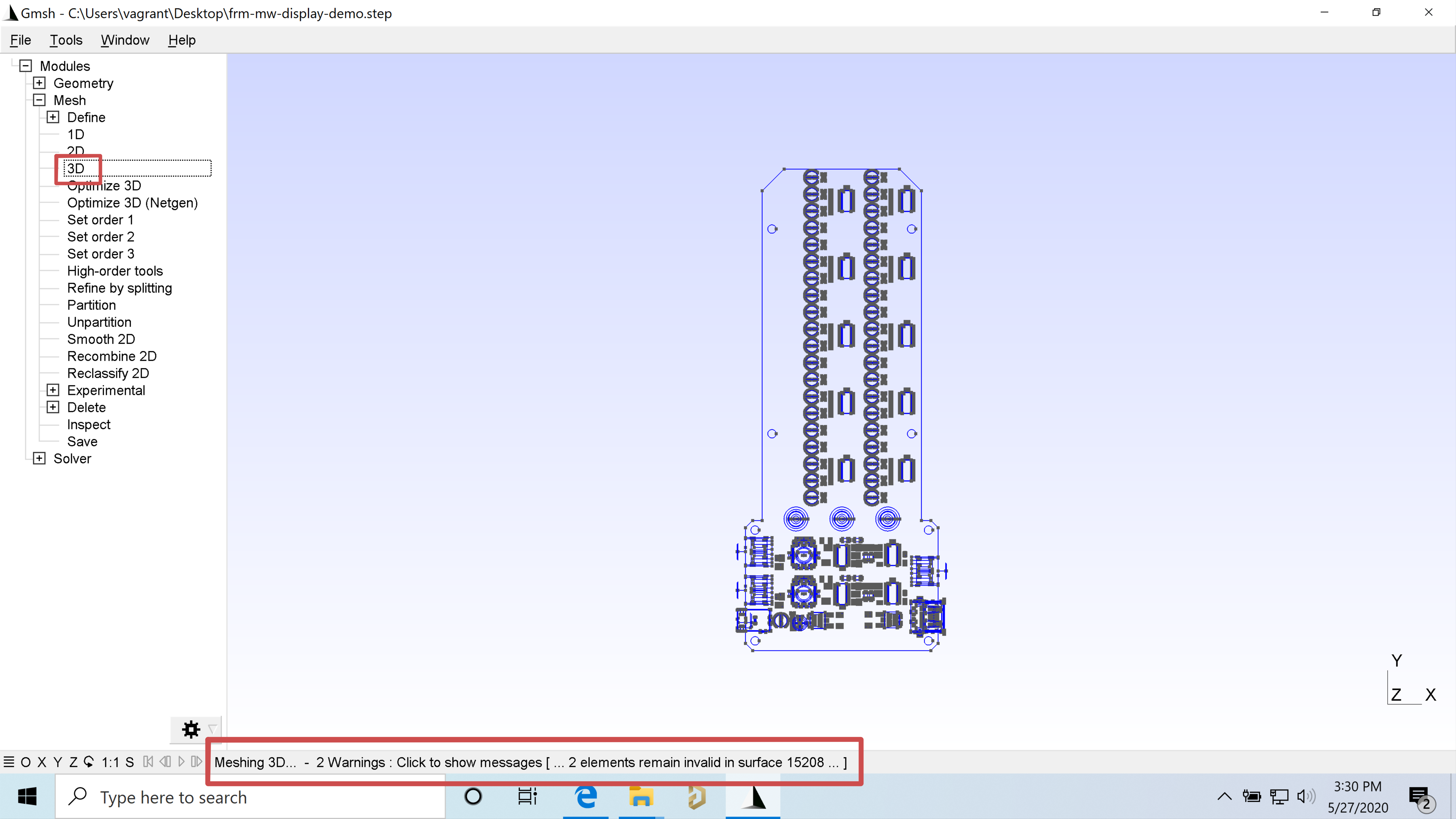
To convert a STEP file to an STL using the GUI, you can follow this process:
- Open the file (file, open). This can take up to 10 minutes
- Run the volumetric meshing. (Modules, Mesh, 3D)
- Save to STL (File, Export)
The meshing process can take a long time, even half an hour for boards with many components.
The status of the conversion is reported on the bottom bar.
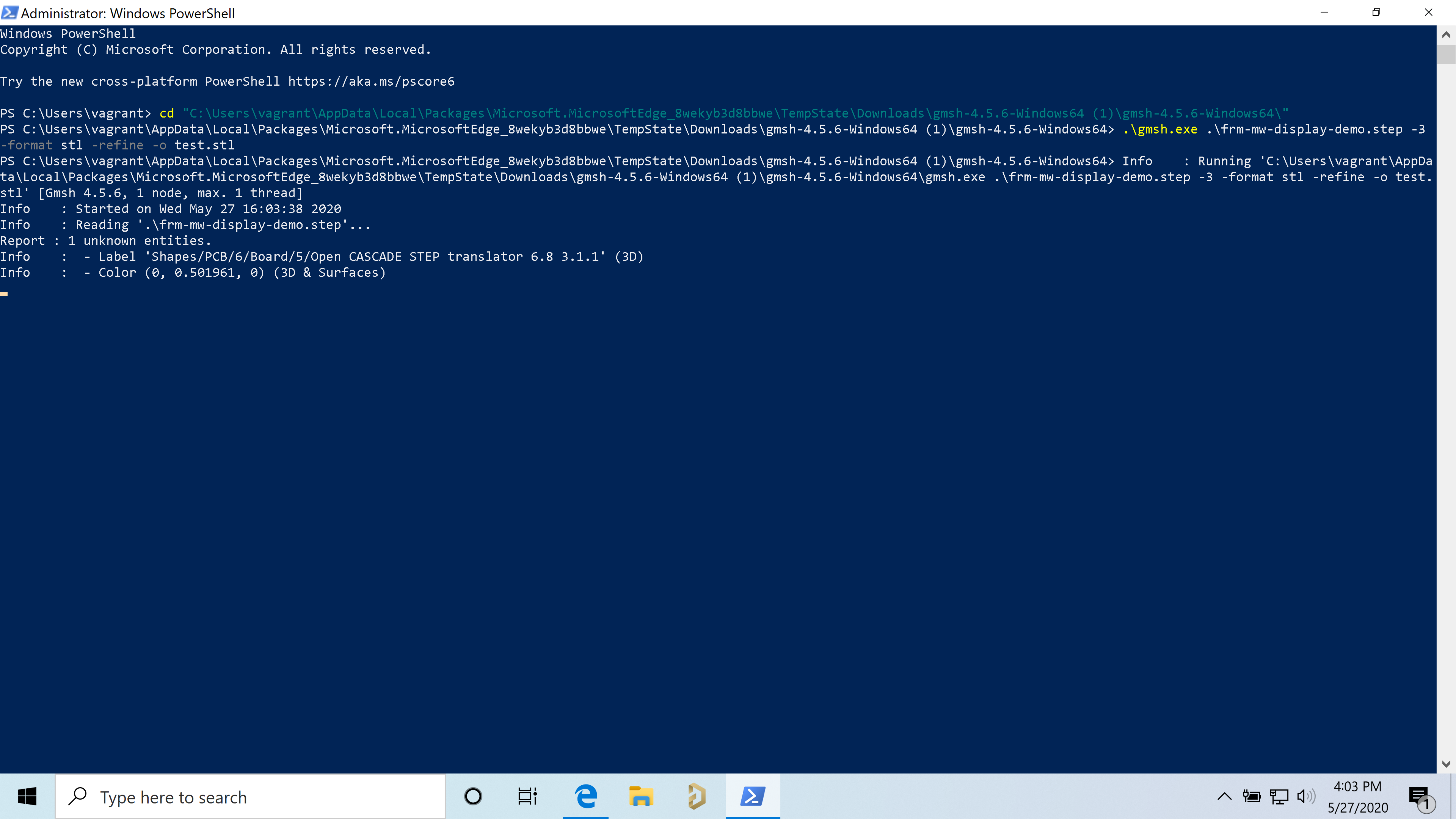
Command Line Usage
Similarly to GUI operation, we can use the command line to perform the conversion, by opening the command prompt into the correct directory issuing the following command:
.\gmsh.exe .\input.step -3 -format stl -refine -o output.stl
The file input STEP file should be placed in the same directory as ghsm.exe for this command to work.
3D Printing Your PCBs
I’m the proud owner of a Prusa MK3, one of the most popular 3D printers on the market. If you see an orange printer that looks something like a maker toy, it’s a Prusa. But it would be best if you did not have yourself made a fool of first impressions; this printer is a capable and well-engineered tool, much more than many of the more industrial-looking counterparts.
.jpg)
The printer has a fully open hardware design and open-source software. The slicer, called PrusaSlicer is among the best in the market. I’ve imported the STL files we have just generated in PrusaSlicer. They’re a bit heavy, but the software handles it gracefully. The STL slices successfully with only a few warnings, mostly about the inability of the printer to create features smaller than the nozzle size.
.png)
Conclusions
When working with the MCAD CoDesigner feature in Concord Pro on Altium 365, it's possible to take your PCB layout and create mesh files for 3D printing PCBs before a prototyping run. Using the free software shown above, you could convert STEP models of your Altium PCB layout to industry-standard 3D printing formats such as STL. This provides a quick and effective dimensional check when your board (including components) is 3D printed as a plastic model.
More advanced 3D printers, such as those from Nano Dimension and Optomec, can be used to print a fully-functional circuit board from STL files. If you go this route, you'll need to export just the bare board as a STEP model and convert it to an STL mesh file to generate printing instructions. Whether you have a 3D printer or not, you can check out the Altium Concord Pro product page to take advantage of integration between Altium 365 and popular MCAD applications like SolidWorks, PTC Creo, and Autodesk Inventor.
Would you like to find out more about how Altium can help you with your next PCB design? Talk to an expert at Altium.