Designing a Custom High Speed Photogate PCB
Slot sized photogates are common in a lot of equipment and machinery, suitable for reading incredibly high count encoder wheels or detecting objects breaking the beam. While they are useful for many applications, commercially available models typically have a slot width less than 2mm. This doesn’t allow you to work with a larger gap to detect a large object.
I’m working on a desktop injection molding machine, and want to detect the part dropping free from the mold cavity. I’d like to have the machine running autonomously and without constant supervision, so ensuring that the cavity is cleared after each injection is vital. If the part is hanging between the mold halves on a string of plastic, or got hung up on the ejection pins, then when the mold halves are closed it could damage the machine.
There’s several options I could use to detect a part falling out of the cavity, but I like the simplicity and reliability of the photogate approach. When used in current conduction mode, the photodiode exhibits an incredibly fast response rate, which allows the smallest parts falling past the sensor to be detected. My problem is, I can’t find a good solution off the shelf that isn’t designed for large industrial machines. The industrial machine parts are typically certified for safety-critical applications, and therefore, are not cheap. My DIY machine needs a solution of sufficient quality, but without getting too crazy expensive.
I intend to have a part chute under the mold body which will allow ejected parts to go into a bin or a box. By having an infrared beam shining from one side of this cavity to a photodetector on the other side, I can detect the part pass-by with a microcontroller. If I connected the photogate to a Schmitt trigger buffer, I could also provide a clean logic level signal into a programmable logic controller or other third party controllers if I wished.
My requirements for this project are fairly simple: detect the absence of light quickly and reliably. Given that the machine might be used with a lot of ambient light around, I want to use an infrared beam, and for the sake of reliability, I intend on using an emitter with a drive current of 100mA. The high drive current of the emitter is more than you would want to use a series resistor to regulate, but probably less than you would want a full fledged LED driver to handle. I like overdoing things though, so I’m going to add a constant current LED driver to the board that can also power the emitter.
As usual with my projects, you can find the schematics and board file on GitHub under an MIT license to use as you wish. The components used in the project are available in my free, open source Celestial Altium Library.
Photodiode
There are many means of measuring light, and photodiodes happen to have the fastest response rate of anything I’ve worked with. There’s a huge difference between using a photodiode in photovoltaic mode vs. using it in current conduction mode. When operating in photovoltaic mode, the diode is a bit like a very poor solar cell and generates a small voltage from the light it’s exposed to. Photovoltaic mode may be fine for basic presence detection applications, but it is not suitable for detecting a high speed event, such as a small part falling past. The junction in the diode has capacitance, which is the limiting factor for the speed of the diode. As the diode receives light, it charges the junction first before giving the expected signal, and when the light source goes away or diminishes, the junction has to discharge before becoming inactive. This capacitance is quite limiting as the voltage and current generated by the photodiode are quite small—too small to charge it quickly.
As an example, if I drive an infrared emitter with my function generator (yellow), we can see the response of the photodiode in photovoltaic mode (blue) on my oscilloscope.
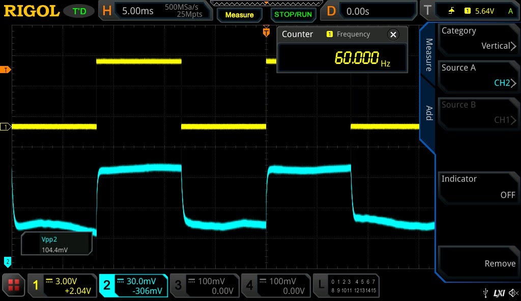
At 60Hz, the waveform is quite acceptable, yet would still need amplification to be usable with any logic device such as a microcontroller.
If the waveform for the infrared emitter is increased to just 1kHz, we can very easily see the effects of the diode junction’s capacitance on its rising and falling edges.
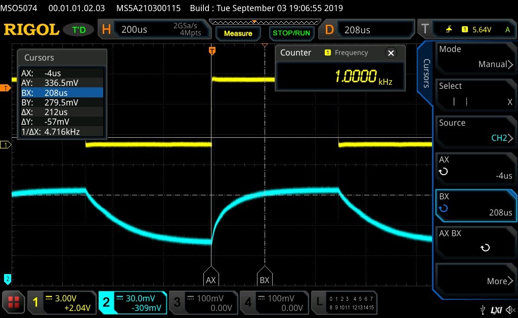
1kHz sounds quite fast, however, if the mold part is quite small, or has tiny features, the duration for which it occludes a narrow infrared beam is going to be short. Given the discharge time of the junction’s capacitance, it might only show as a slight blip and not be detected.
Because of this delay, we need a better way to use the photodiode. I mentioned earlier it has a very high speed response, and this is true in current conduction mode. With the diode reverse biased (cathode connected to positive voltage), the junction will begin to conduct current almost immediately upon light hitting it, and stop almost immediately upon that light going away. This allows the detection of even slight interruptions to the light source.
Here is the same photodiode and emitter pair running in current conduction mode—through the transimpedance amplifier we’re going to build in this project.
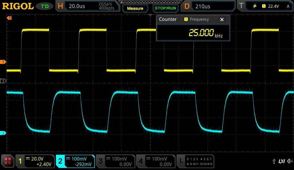
With a 25kHz signal, there is some rounding to the rising and falling edges, but it is a vastly superior waveform compared to the 1kHz signal from the photovoltaic mode. As a note, the little spikes on the waveform are caused by the circuit picking up and amplifying noise from my cheap LED magnifying lamp (which I struggle to believe meets the EMI requirements of a CE mark, based on the noise it radiates).
Given that we will need to amplify the signal from the photovoltaic mode diode, and we can use the same components of the photovoltaic mode’s amplifier to build a transimpedance amplifier for the current conduction mode, it makes sense to just use the diode in current conduction mode and build the transimpedance amplifier!
Transimpedance Amplifier
If you’ve read my other project articles, you know I love a good online calculator. To provide a starting point for the transimpedance amplifier design, I used Analog Devices Photodiode Design Tool. It’s a great tool, but it really only works as a starting point. Given that I’m optimizing for a square edge on a potentially very short duration pulse, my final values varied significantly from those which the online calculator generated. It’s always great to have a starting point for a project though. The calculator yields some values that can get you going in the right direction, so it’s still a great tool to begin your design with.
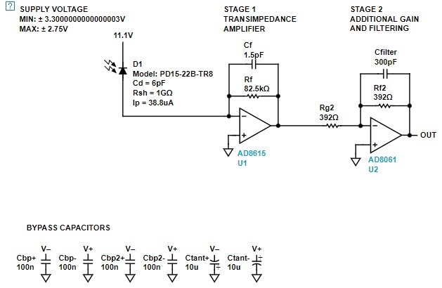
Using the schematic generated by the design tool, I populated out a breadboard with these parts, except I used a multi-turn potentiometer instead of fixed value resistors. Using the function generator to drive the LED with the oscilloscope hooked up to the output of the amplifier allows for the rapid tuning of the circuit.
To power the circuit, I’m using my benchtop power supply to provide 12V to the diode, and a linear adjustable voltage regulator set to output 2.75V for the positive rail of the op amps. I also have an inverting charge pump to provide the -2.75v required for the negative rail of the op amps. When working with just tens of microamps of current from the photodiode, an op amp referenced to ground isn’t suitable. The op amps can generate output voltages no less than a certain threshold above their VEE terminal, which means grounding the VEE terminal will prevent them from generating very small values of output. Instead, connecting a negative voltage allows the op amp to generate signals as low as 0V, thereby allowing us to work with smaller signals. These days, not all op amps are capable of working with a negative voltage, so care is required with op amp selection. Of course, the Analog Devices design tool suggests a suitable selection of op amps that will work well with the small current and high frequency requirements. This, to my thinking, is the primary value of such a design tool: saving us from hours of reading datasheets just to rule a potential op amp as valid or not.
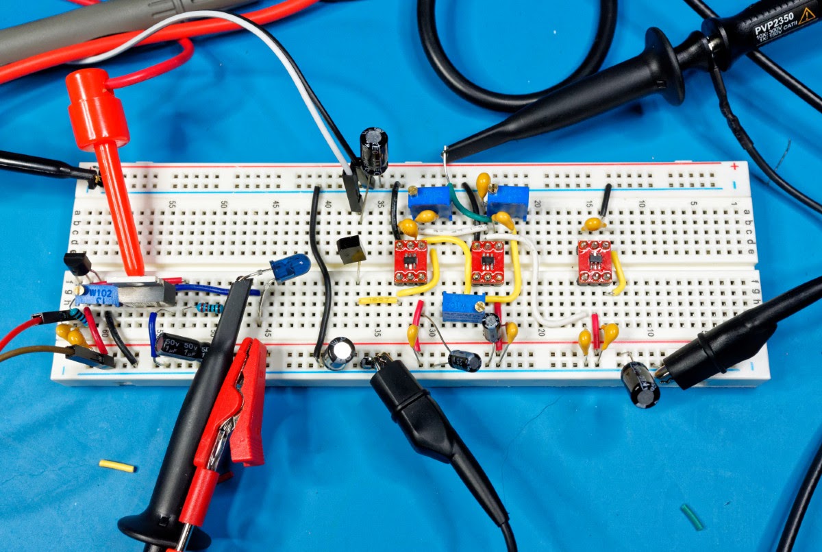
Tuning the circuit is an iterative process. Adjust the first op amp’s feedback resistor to start squaring up the waveform, then move to the middle resistor, then the feedback resistor on the second op amp. Repeat this until the waveform starts to look good. I found that the capacitors in parallel with the feedback resistors were limiting my progress with the tuning. I started switching out the capacitors with progressively smaller values until I wasn’t able to optimize the circuit any further.
This optimization process will be highly dependent on your photodiode model and the emitter that is activating it. The distance the emitter is from the diode has a large impact on the circuit tuning. You should tune the circuit with the emitter powered as it would be in your final application, and at the same distance, or alternatively, scale the emitter power down and use it closer as I have. I’m using the emitter at a fraction of its rated power to emulate the amount of light the photodiode would receive at the distance I intend to use it at.
Once the circuit looks good, you can pull the resistors out to measure them with a multimeter. The values are likely to be large enough that a simple 2 wire measurement is going to be sufficiently accurate. Once you have the tuned values, you can substitute in the closest orderable (1%) values and check that the performance is still sufficient.
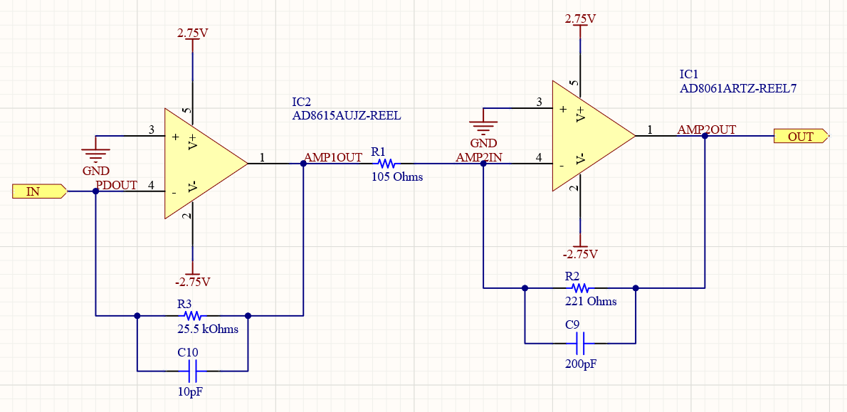
If you compare this schematic with the one that was generated, you’ll notice that my values are significantly different from the design tool suggested I start with. The new values provide a much more responsive circuit that is still stable and has a clean output.
Power Supplies
When working with such small signals, we need to ensure the power supply is very stable and well filtered. If you were looking to use the analog output of the transimpedance amplifier for measuring light levels, rather than using it as a logic output as I am, you could consider using voltage references to power the circuit instead of a linear regulator. The op amps draw a small enough current that a voltage reference wouldn’t have a problem providing a stable and precise voltage to them.
To reduce cost, however, I’m going to make do with a linear regulator, which will be more than good enough for most applications.
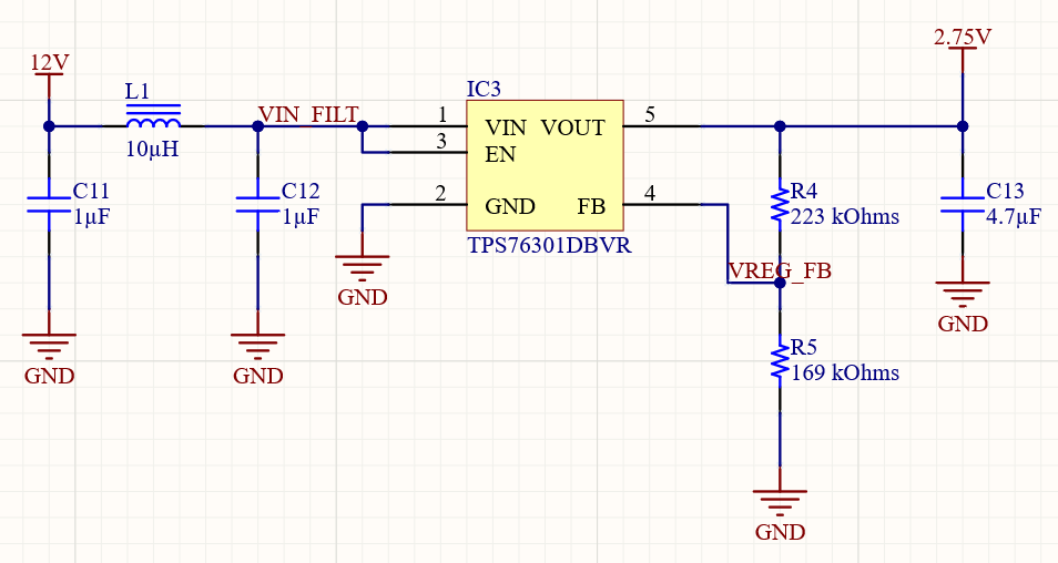
My 2.75V power supply is a basic adjustable linear power supply, with a small Pi filter on the input. I didn’t calculate the cutoff frequency of this Pi filter, I just used values that looked good—basically as large an inductance value as I could get in the package size I wanted to use without the cost or DC resistance getting too high. I could also have used a ferrite for the input. I don’t know what frequency of noise might be conducted into the circuit from the 12V input, so it’s tough to design a filter specifically to cut that noise from the supply.
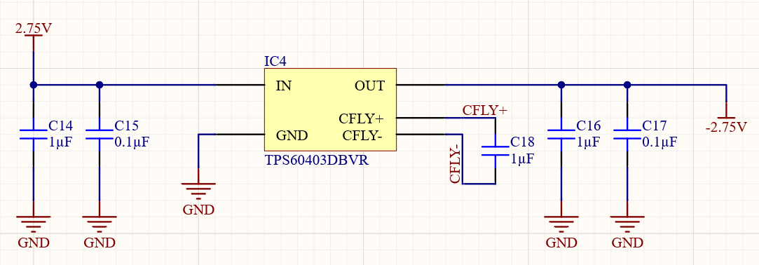
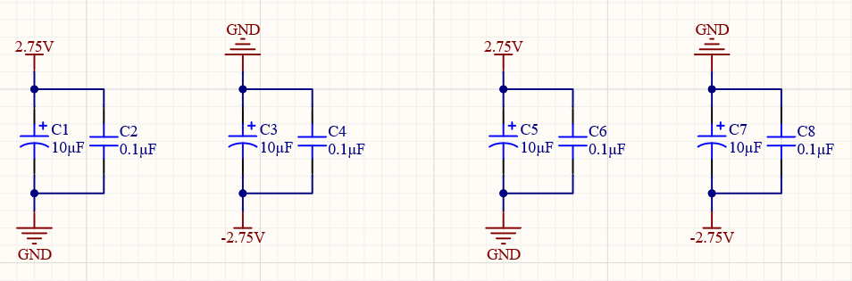
For the negative voltage, I’m using a low cost inverting charge pump. It is only capable of supplying a small amount of current, however the op amps have a very low draw which makes this regulator more than capable of powering both of them. The inverting charge pump creates voltage that is the inverse of the voltage it is supplied, with no regulation. Because of the way it works, it is a fairly noisy supply, which is why I have the 10μF tantalum polymer bypass capacitors for the transimpedance amplifier op amps.
Emitter Driver
I mentioned earlier in the article that I needed a constant current source for the IR emitter, and there are simple ways to do this for a 100mA emitter. However, I wanted to use a full LED driver for this. It is a more expensive option, but I felt bad for the abuse I gave the TPS92512 in the 65W LED Driver project. It’s a great driver IC, and relatively low cost for its capabilities, so I wanted to give it a chance to be in a project where it wasn’t being pushed to its absolute limits. Therefore, I built a 120mW driver around it, quite a change from its previous duties!
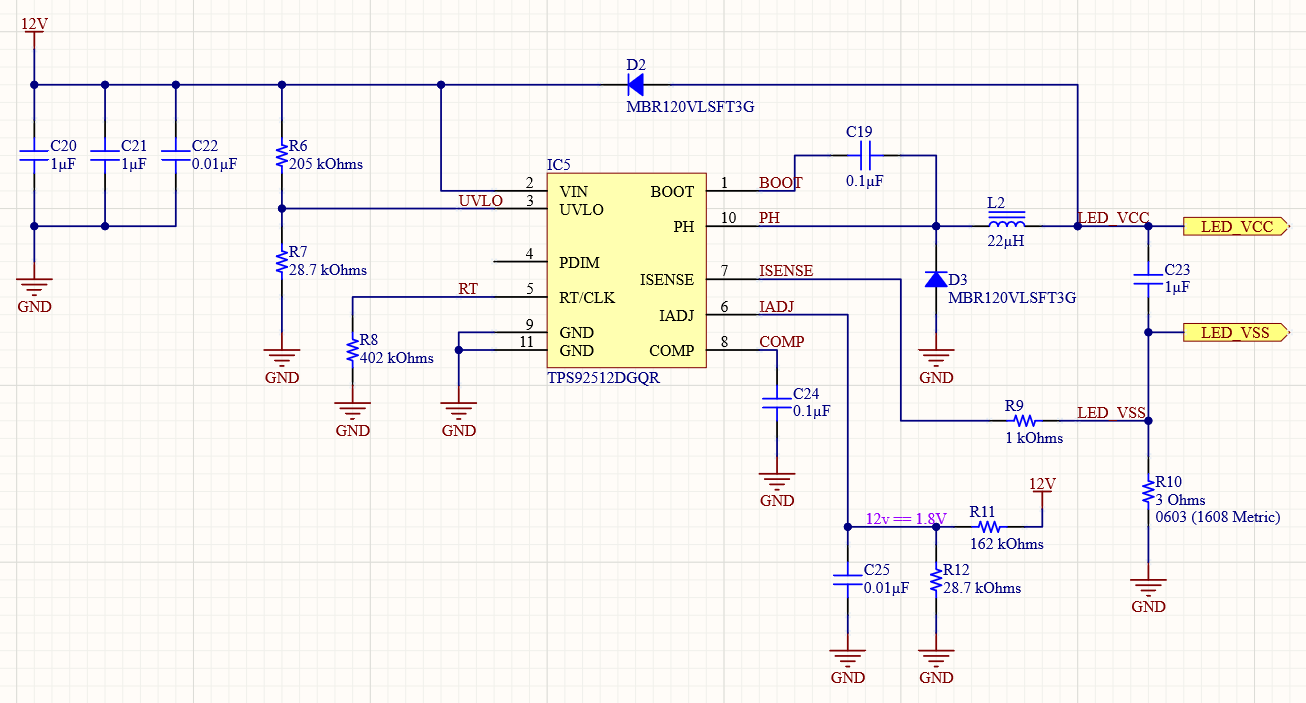
If you want to read about the design process for this driver, you can see my write-up in the 65W LED Driver project. The process for designing this driver isn’t much different except I’m only driving 1.2V and 100mA on the output.
This driver should provide a stable illumination for my photodiode, ensuring there are no false triggers. A driver that uses PWM output to achieve a constant average current on the emitter will not be suitable for a well tuned photodiode. The photodiode’s response should be fast enough to cause your logic to fire on every PWM pulse, which would make the firmware development far more difficult than it needs to be, or require hardware hacks that would reduce your response rate to an actual event.
If your photogate only needs a small gap, you can likely use a much lower power IR emitter and use a series resistor for current limiting, as you would with any low current discrete LED. My application requires a large gap, and therefore a more powerful emitter, to ensure enough light is going to hit the sensor to produce a good signal from the amplifier.
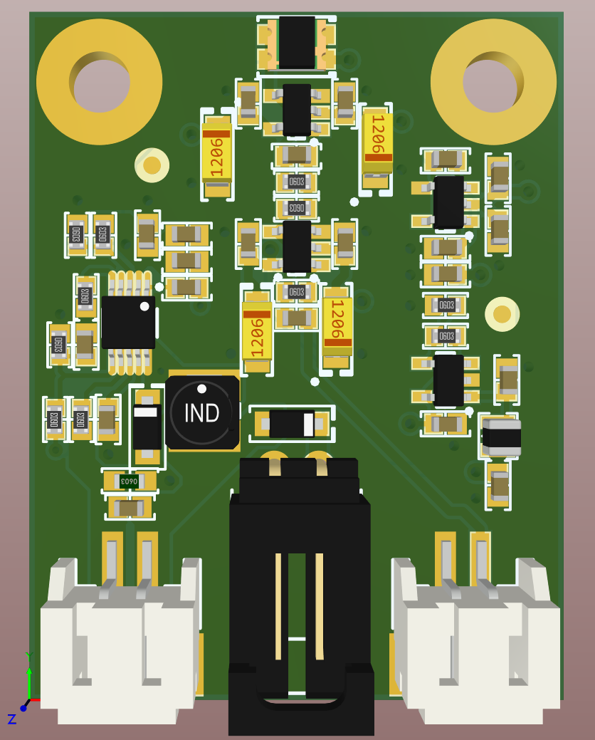
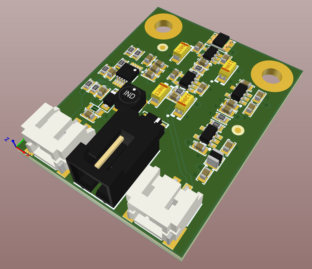
Board Layout
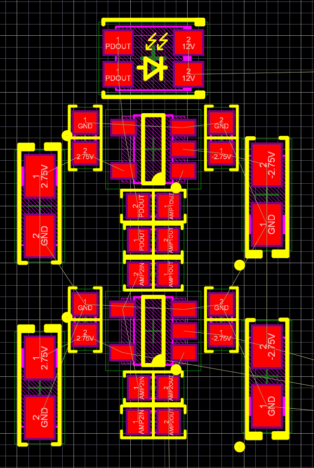
I’m starting the board design with a rough layout of the transimpedance amplifier. I’d prefer a long, narrow layout, as it should allow me to keep the relatively noisy switched-mode emitter driver as far away from the small signals of the photodiode as possible. The less noise the photodiode picks up, the better.
The layout keeps all the signals in this very sensitive chain as short as possible. Earlier in the article, I had a screenshot from my oscilloscope with noise that was picked up from my LED magnifying lamp. That lamp was almost half a meter away from the board when the screenshot was taken—the noise may have been picked up by the oscilloscope probes, or it may have been picked up by the wires or even the breadboard itself. Either way, it shows how sensitive the circuitry on an amplifier working with such small signals is. By keeping the traces as short as possible, we can reduce the amount of EMI that is able to be coupled into the amplifiers.
I have added the power supplies for the amplifiers off to one side. In hindsight, I probably should have placed the inverting charge pump IC where the linear regulator is in order to move its switching noise further away from the photodiode. If this was a board I was going to make more than one or two of, I would likely have taken the time to do this, however for the application I have in mind, I don’t feel as though it will be an issue—certainly not a large enough issue to warrant a second set of prototypes being made.
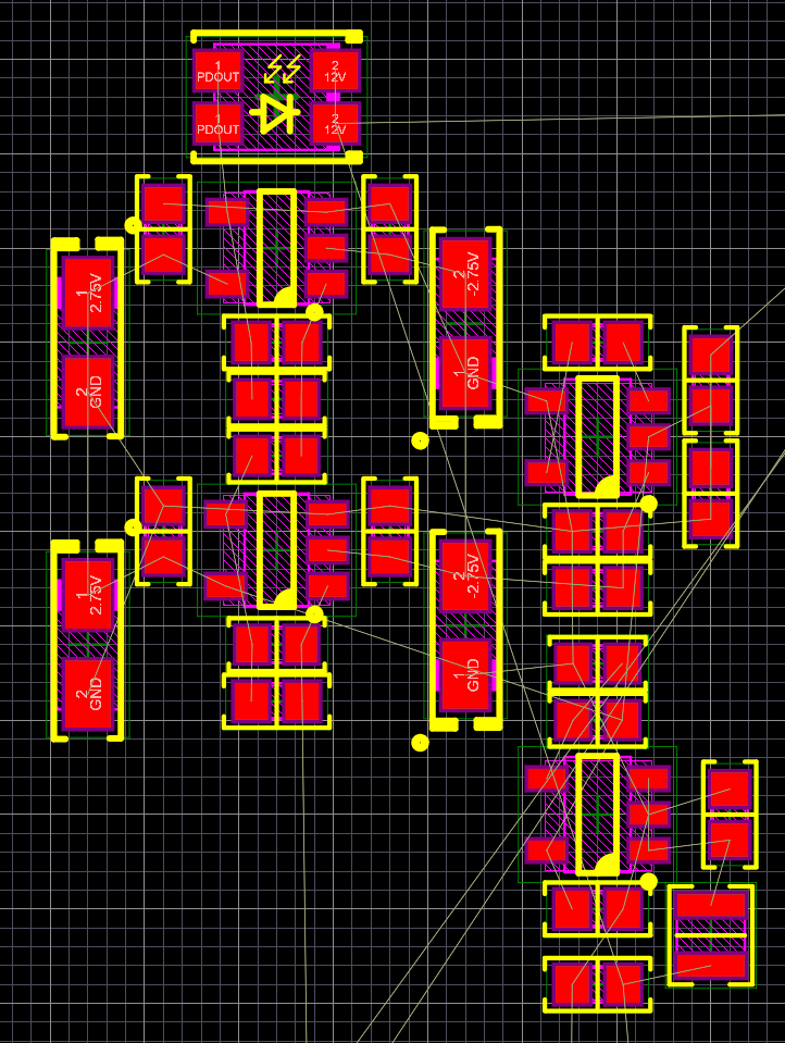
Next, I’ve tried to place the emitter driver as far away from the photodiode as possible without making the board too big. The connectors at the end provide a minimum board width, which I’ve allowed to grow a little larger. This is just a first pass rough layout; more of an idea of what I’d like to see. The component placement will change as we actually route the board.
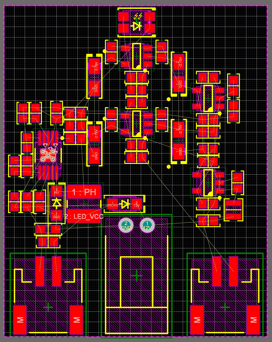
Many of my recent projects started out by routing with massive polygon pours. It’s nice to be doing the routing on this board with actual traces! The current on this board is small enough that I only need to use polygons if I want to, rather than being forced to by the high currents.
I decided to start with routing the emitter driver. Its layout is very similar to the high power one I previously designed, but more compact from the much smaller components which the lower power allows. I started with this section of the board as I feel it’s the most likely to have the layout shuffled around and perhaps need a bit more space on the board, which would affect the size or overall layout requirements for the board. The transimpedance amplifier, on the other hand, is relatively simple with the signals flowing across the board in a sensible fashion.
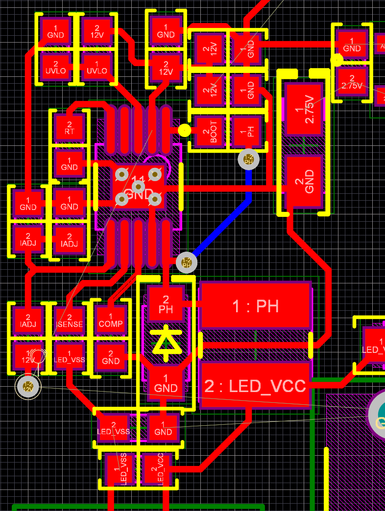
Once the driver was routed and its layout shuffled around a bit to make room for traces, I was able to route the rest of the board very easily. I added a couple of polygons for the emitter driver, the current density doesn’t require it, but the polygons for the switching nets should help reduce noise.
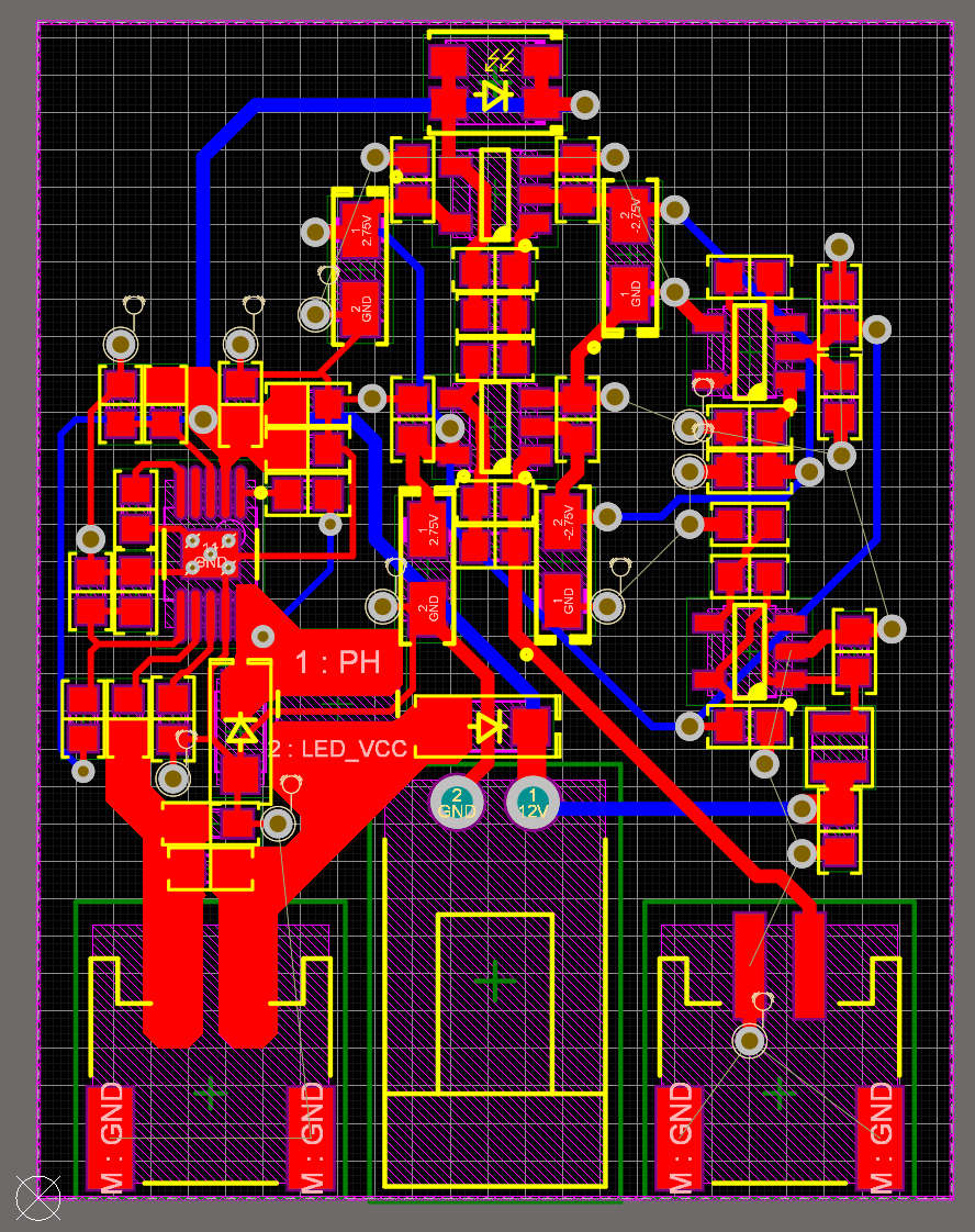
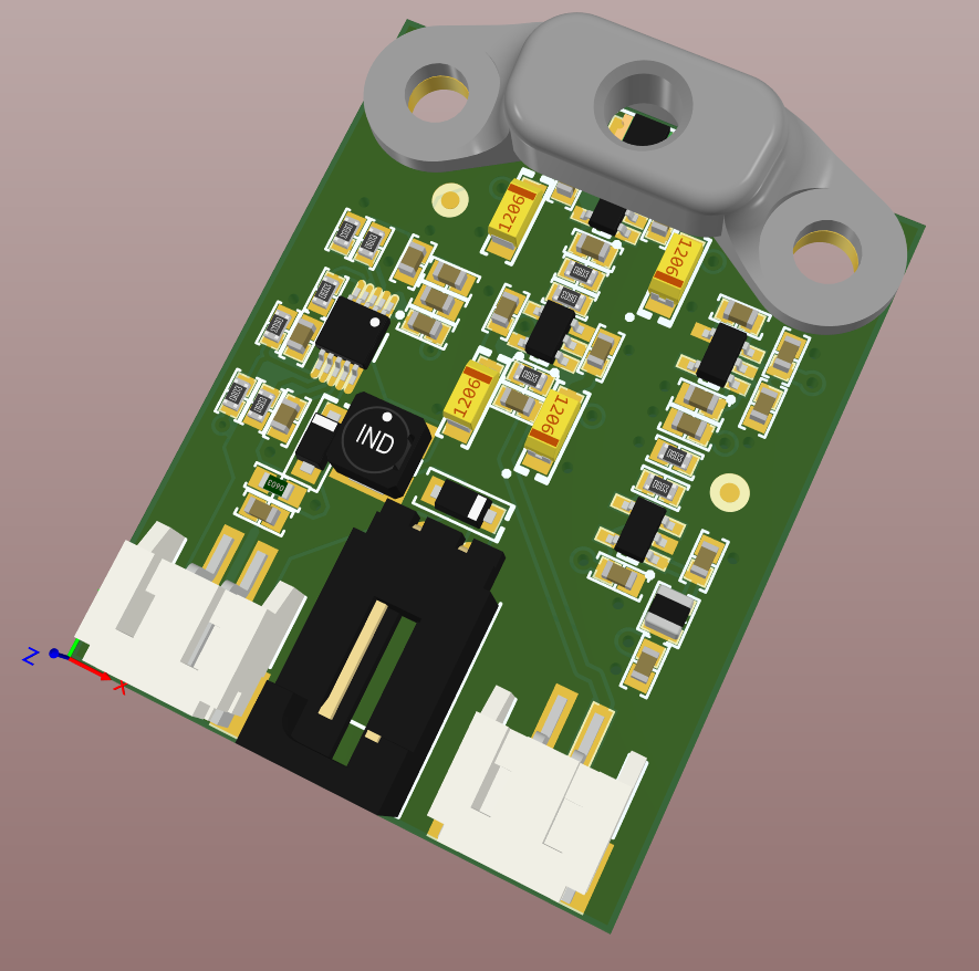
Finally, for the board layout, I added fiducials and M3 mounting points to the design. The fiducials are required for machine assembly and the mounting points will be used to attach a shroud to the board.
The emitter doesn’t require its own board. Through-hole IR emitters tend to have much narrower beam widths, as they have a lot more room for the lens than a surface mount option, and the narrow beam width is perfect for my application. The emitter will simply be soldered to wires that terminate with a connector plugged into the photogate board.
Photodiode Light Shroud
To prevent stray or reflected infrared light from making its way around the parts I’m looking to detect and hitting the photodiode, I want to design a simple shroud to mount on the board. The mounting holes I added earlier will work well for securing the shroud as well.
I don’t have a Solidworks license, or licenses for any of the other high end CAD packages that Altium supports. This means I’m not able to use the amazing MCAD-ECAD integration that Altium provides, a functionality that got even better in AD20!
I’m going to use Fusion360 to build the shroud for the photodiode, and the easiest way to get the board into Fusion is with the STEP export. The Parasolid model is far more detailed—however, that just causes performance issues for Fusion. If I was looking to make photorealistic renders, the Parasolid would be the way to go.
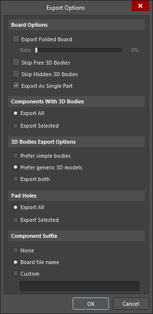
To generate the STEP model of the board and components, we can go to File -> Export -> STEP 3D.
When you add the STEP model to Fusion, it will be uploaded and processed. This is pretty quick and the file is available in short order. One of the reasons I put so much effort into the 3D bodies for my Altium Database Library is for situations like this, where I want to build a mechanical part onto the board without worrying about components clashing in production because a generic 3D model was used, rather than one that was exactly the size specified by the manufacturer.
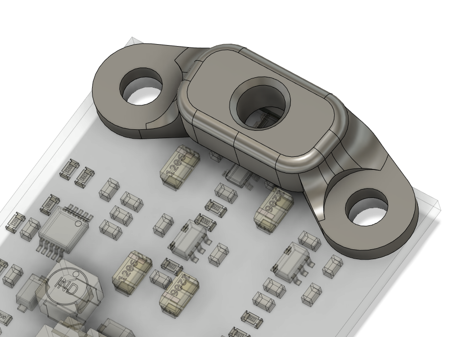
My shroud is relatively simple, and light could certainly make it through the small gap over the first amplifier. Nevertheless, it will greatly reduce the amount of light that could make it to the sensor from an unwanted direction. If light entry from the bottom of the shroud proves to be an issue, a quick shot of black hot melt glue will seal that gap up in a hurry!
Once the shroud design was complete, I exported a STEP model of the body and imported it into Altium Designer to check the position and fit. Altium Designer’s component clearance checks are much easier to use, and more obvious than those built into any mechanical CAD package I’ve used!
The shroud is simple enough that it should be easy to print with a filament-based 3D printer, or a resin printer for an injection molded look.
Finally
Careful tuning is important to get optimal performance out of a photodiode-based high speed photogate design. A little work on a breadboard using the photodiode and amplifiers you plan on using is well worth the effort, as calculated values might end up being inappropriate for your design when it comes to real world application. The amount of light hitting your photodiode is a major influencing factor in component selection, and one which is hard to determine in a simulation.
You can find the complete Altium project for this design on GitHub along with all my other projects.